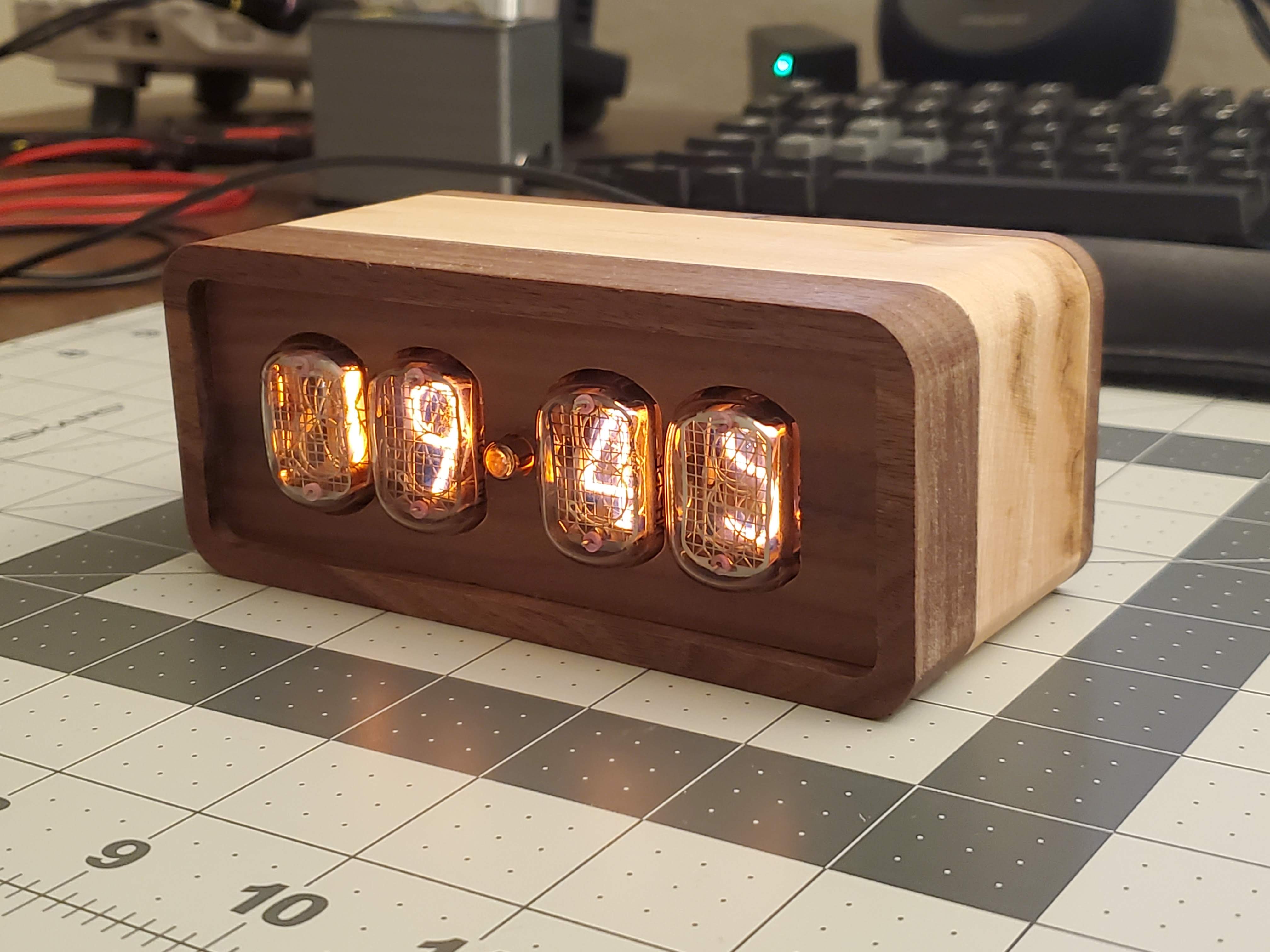
Nixie Tube Clock
2022Github: https://github.com/kevinbchen/nixie-clock
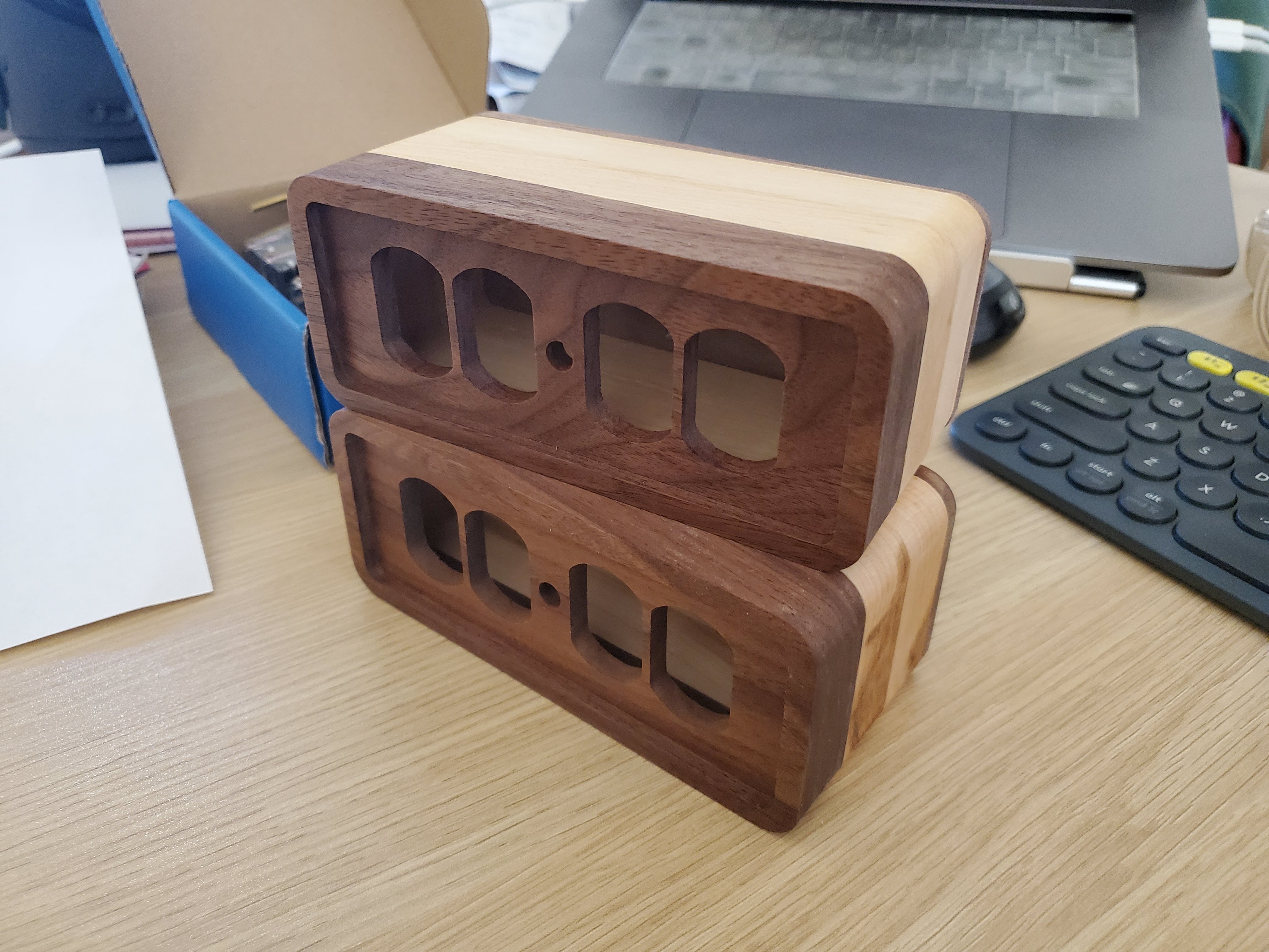
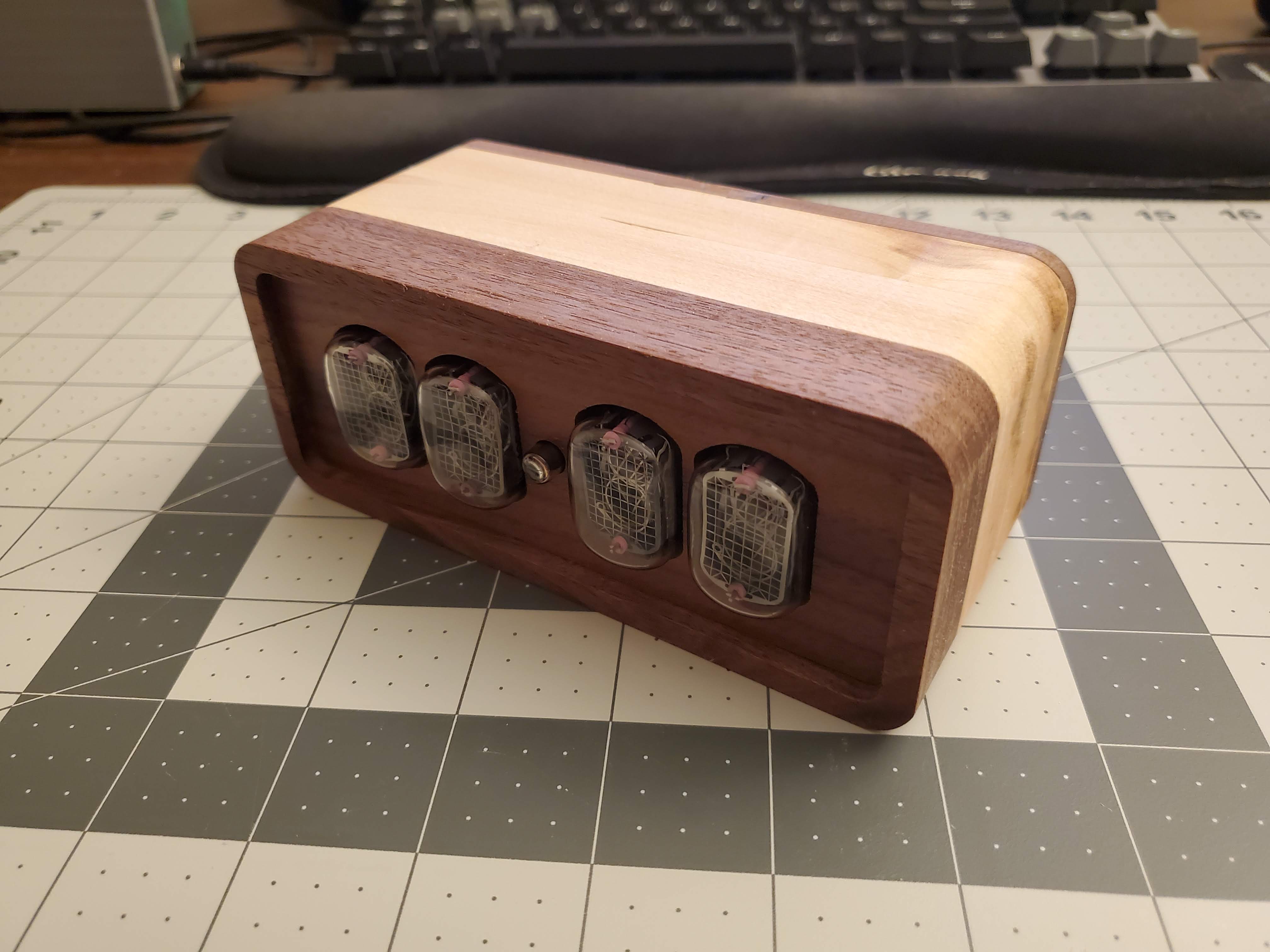
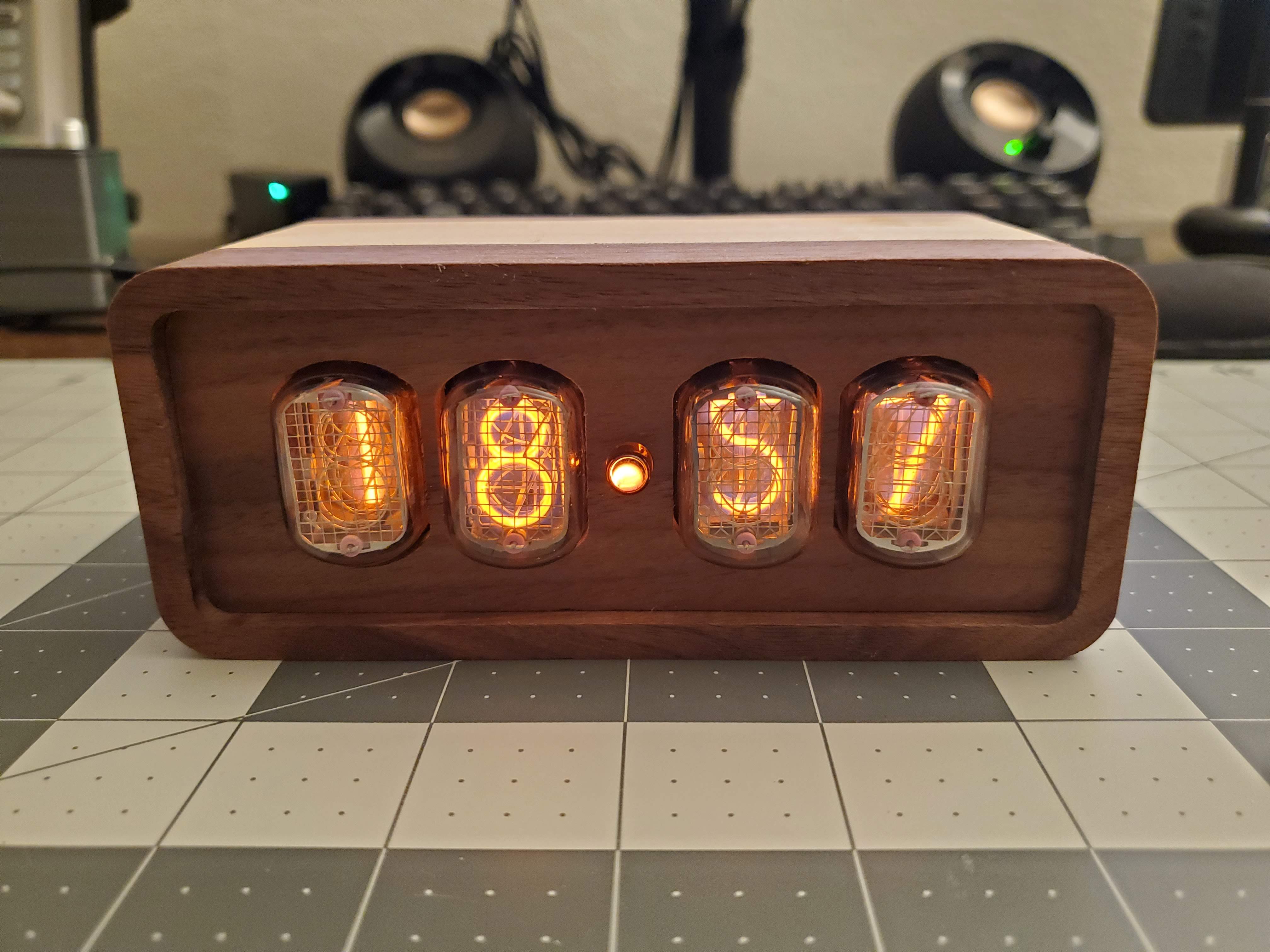
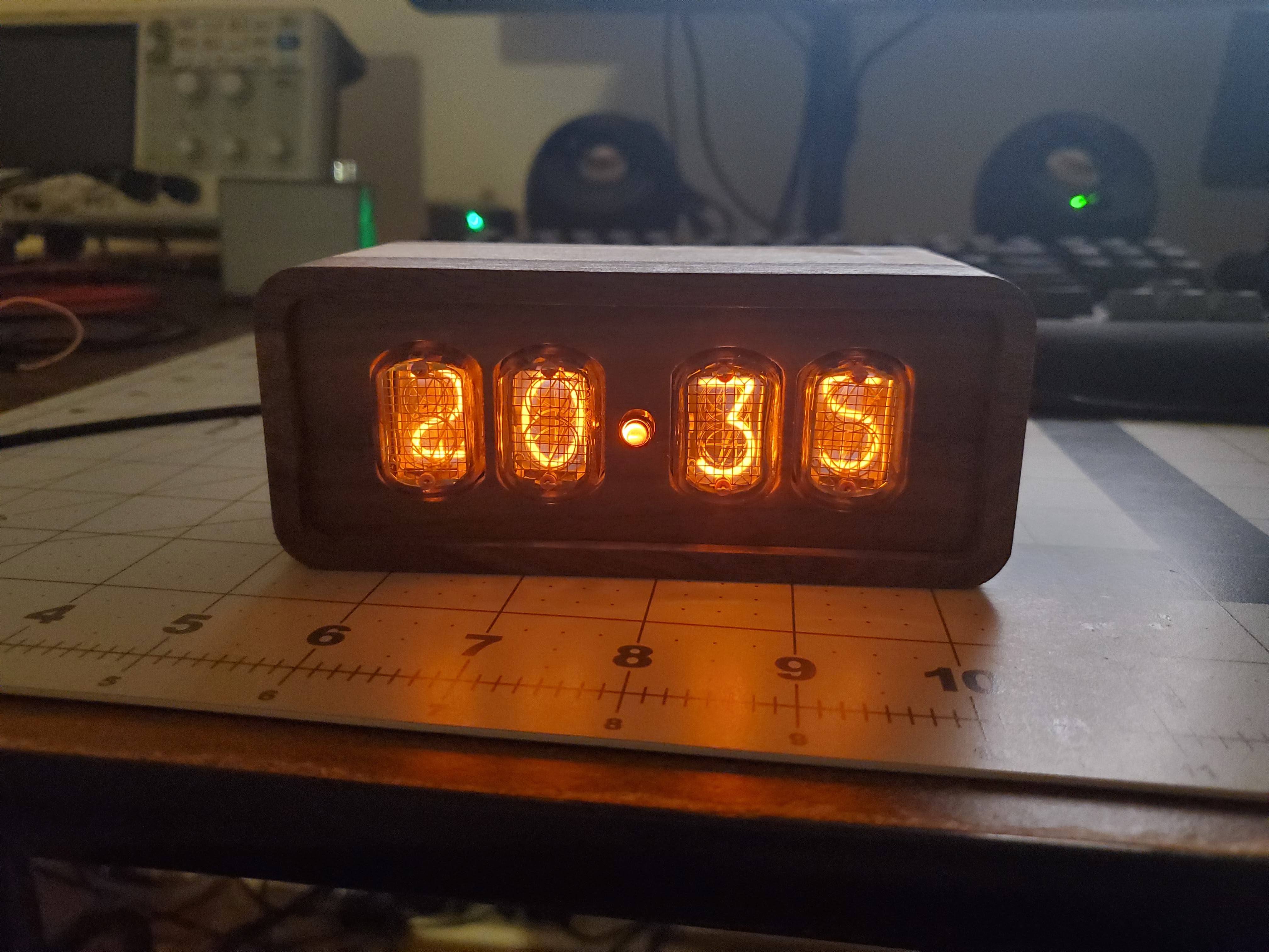
This is my take on the ever popular nixie tube clock. It’s a pretty simple design featuring four IN-12B nixie tubes in an enclosure made of maple and walnut. I designed and built the clock from scratch, though I referenced and took inspiration from a number of other nixie tube clocks on the internet.
I had a lot of fun on this project, and I learned quite a bit on both the electronics and woodworking side!
Electronics
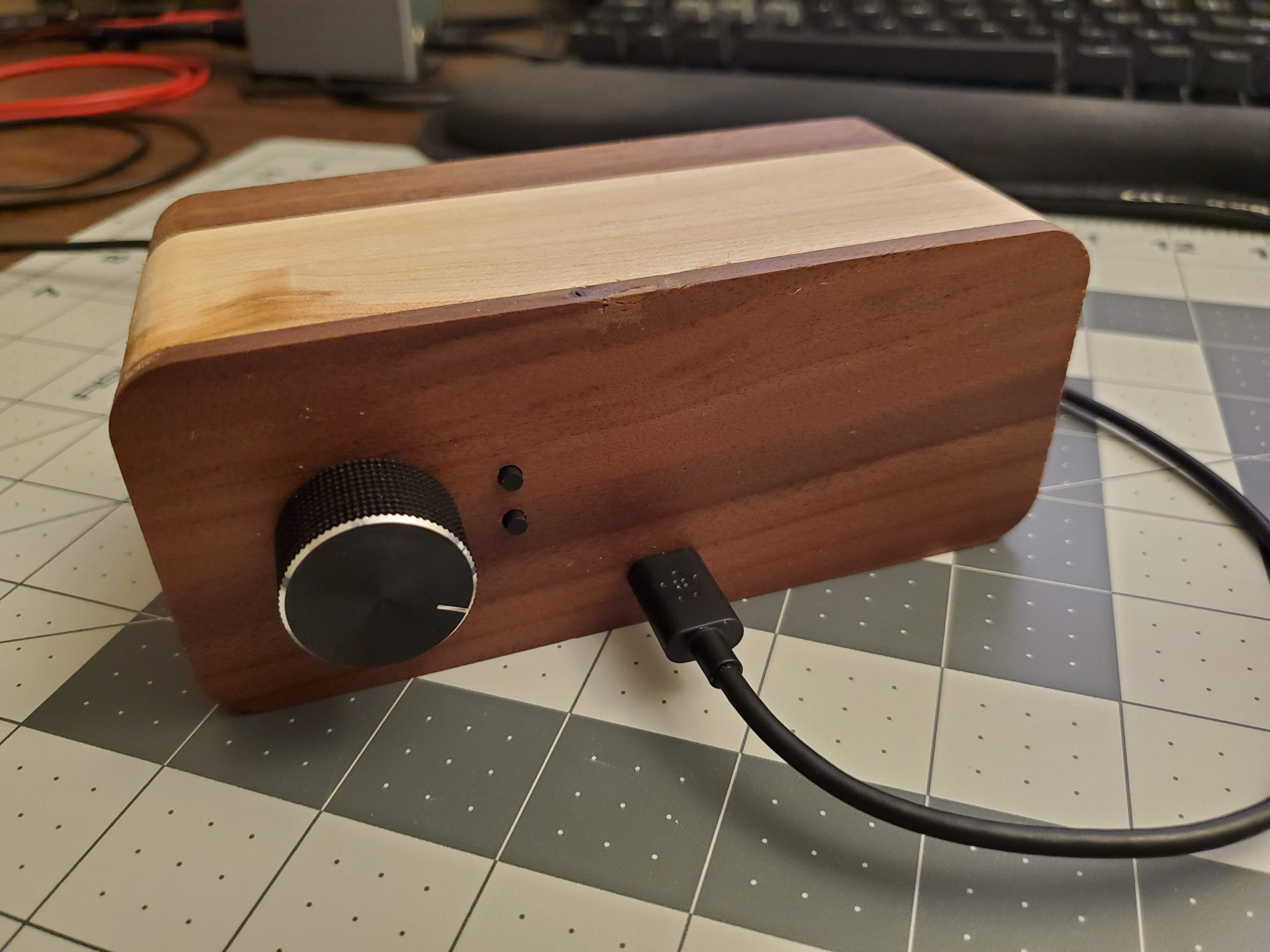
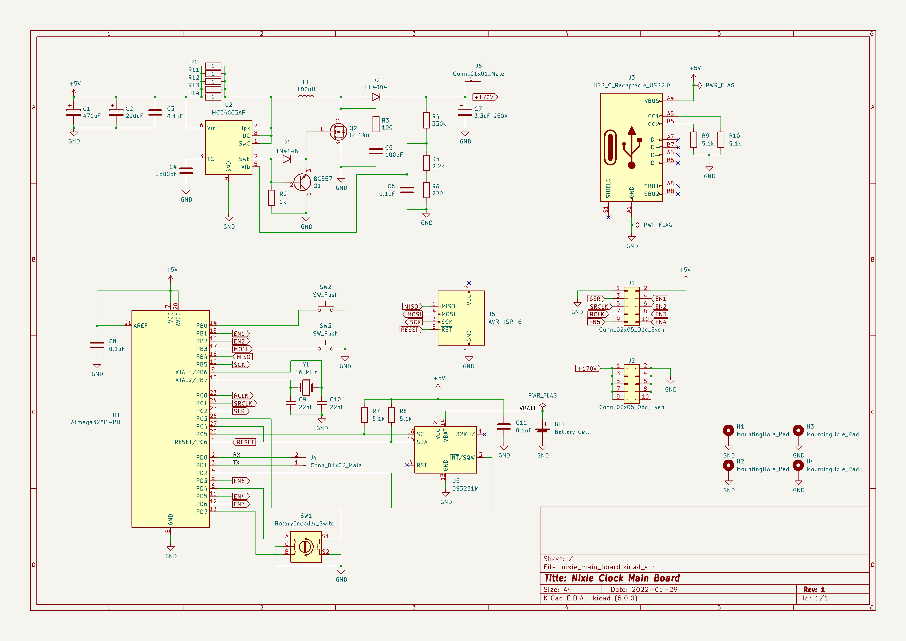
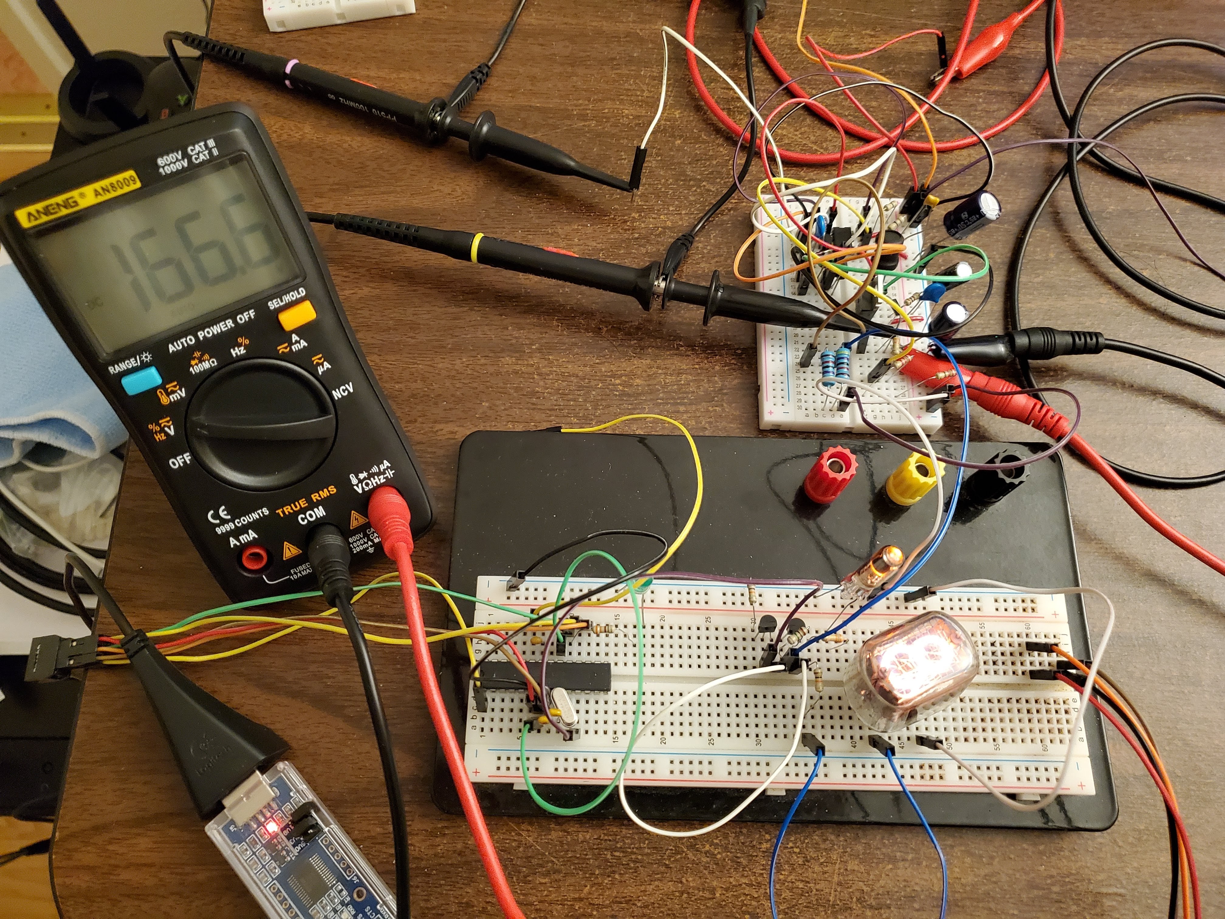
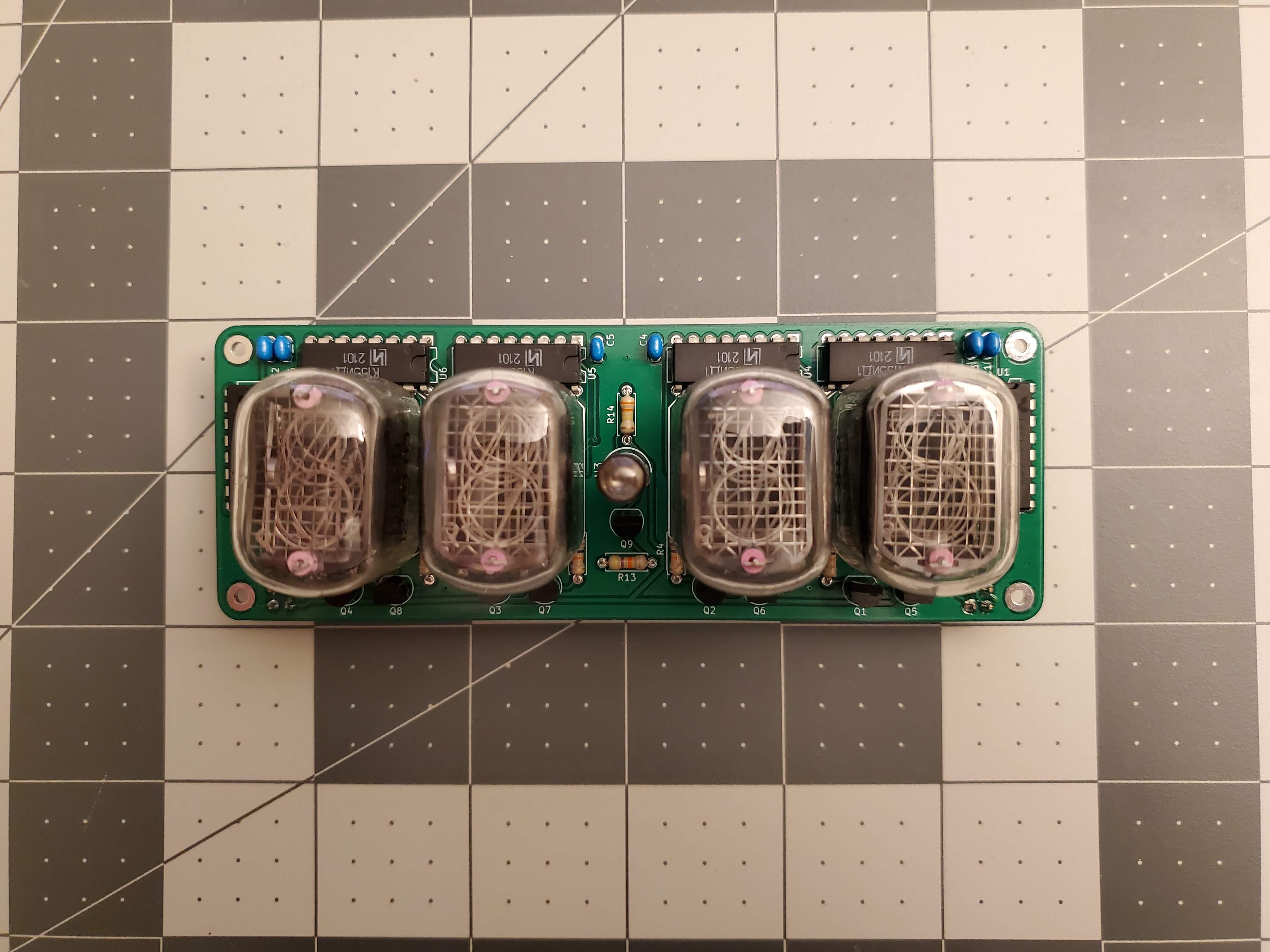
The clock’s display consists of four IN-12B nixie tubes and an INS-1 neon bulb for the middle separator dot. The digits are driven via K155ID1 chips (not multiplexed), and each tube’s brightness can be adjusted individually via PWM. Power is supplied via USB - the clock has a USB-C connector for convenience, but only uses 5V (no power negotiation). A boost converter steps up the 5V to ~165V to power the nixie tubes.
The clock uses an ATmega328P as the main microcontroller and a DS3231 RTC chip for timekeeping. A CR3032 battery is used to keep time in case the clock loses external power. The DS3231 is convenient because it requires minimal external components (it includes an internal crystal) and has good accuracy (+/-2ppm).
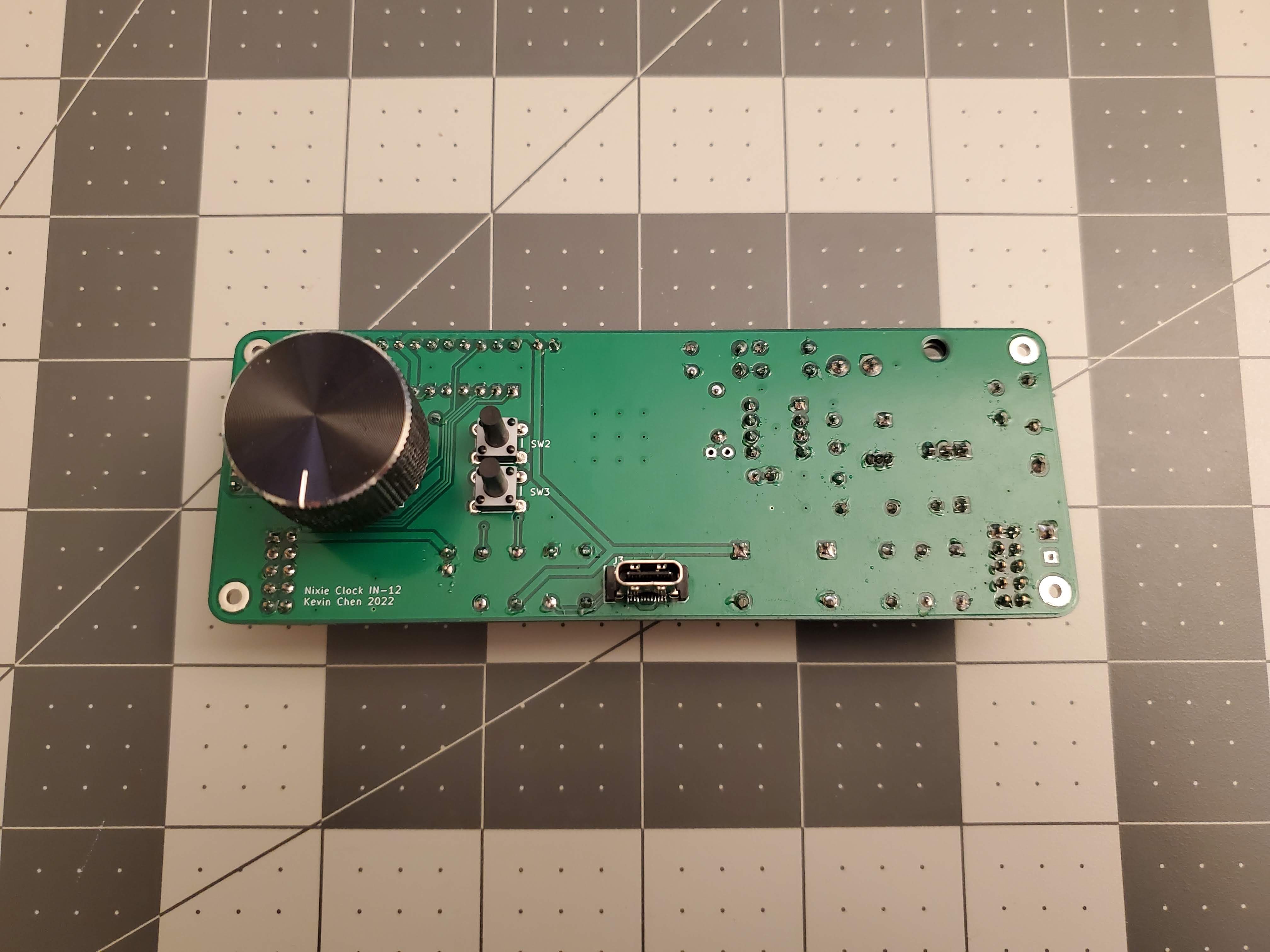
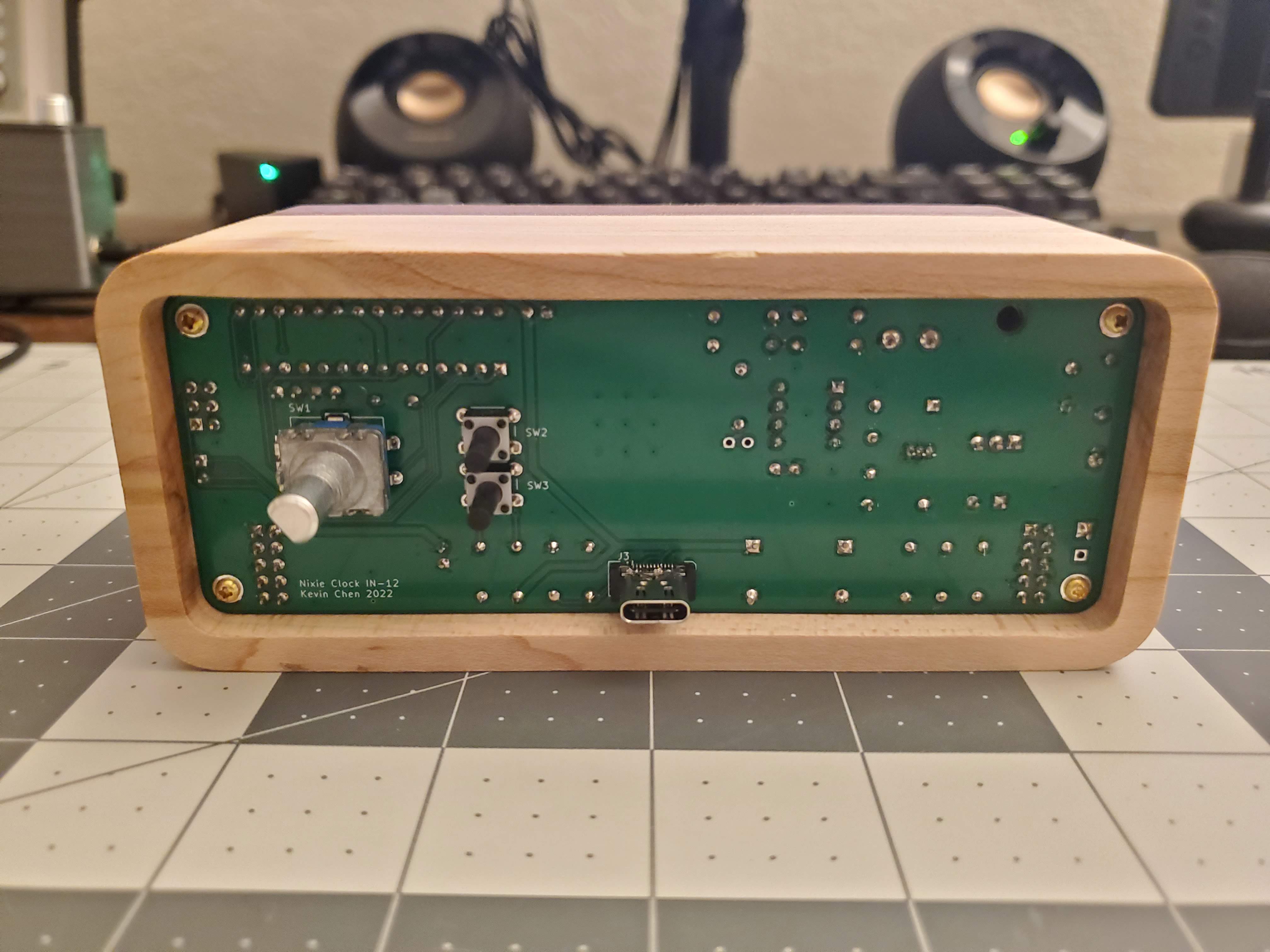
There are 2 pushbuttons and a rotary knob for input; these are used to select the clock’s display (year, month/day, hour/minutes), and to adjust settings.
High Voltage Boost Converter
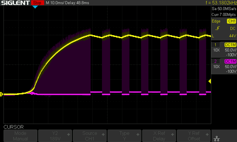
Nixie tubes are interesting because they require a relatively high voltage - typically 170V for the initial “strike” and then 130-150V to maintain the glow. I wanted to power the clock with 5V from USB, so I needed to build a boost converter to step up 5V to 170V. Prior to this project, I had only worked with common digital voltages (3.3V, 5V), so building a circuit to generate such a high voltage was a bit daunting.
At its core, a boost converter consists of a switch, inductor, diode, and capacitor. As the switch is toggled, the inductor alternately stores energy and releases it at a higher voltage. The capacitor is charged to this higher voltage through the diode and continues powering the load while the inductor is storing energy. The basic idea isn’t too hard to understand, but there are a ton of details related to component selection and minor adjustments that make power supply design much more complex in practice. I know I only barely scratched the surface during this project.
555 Timer
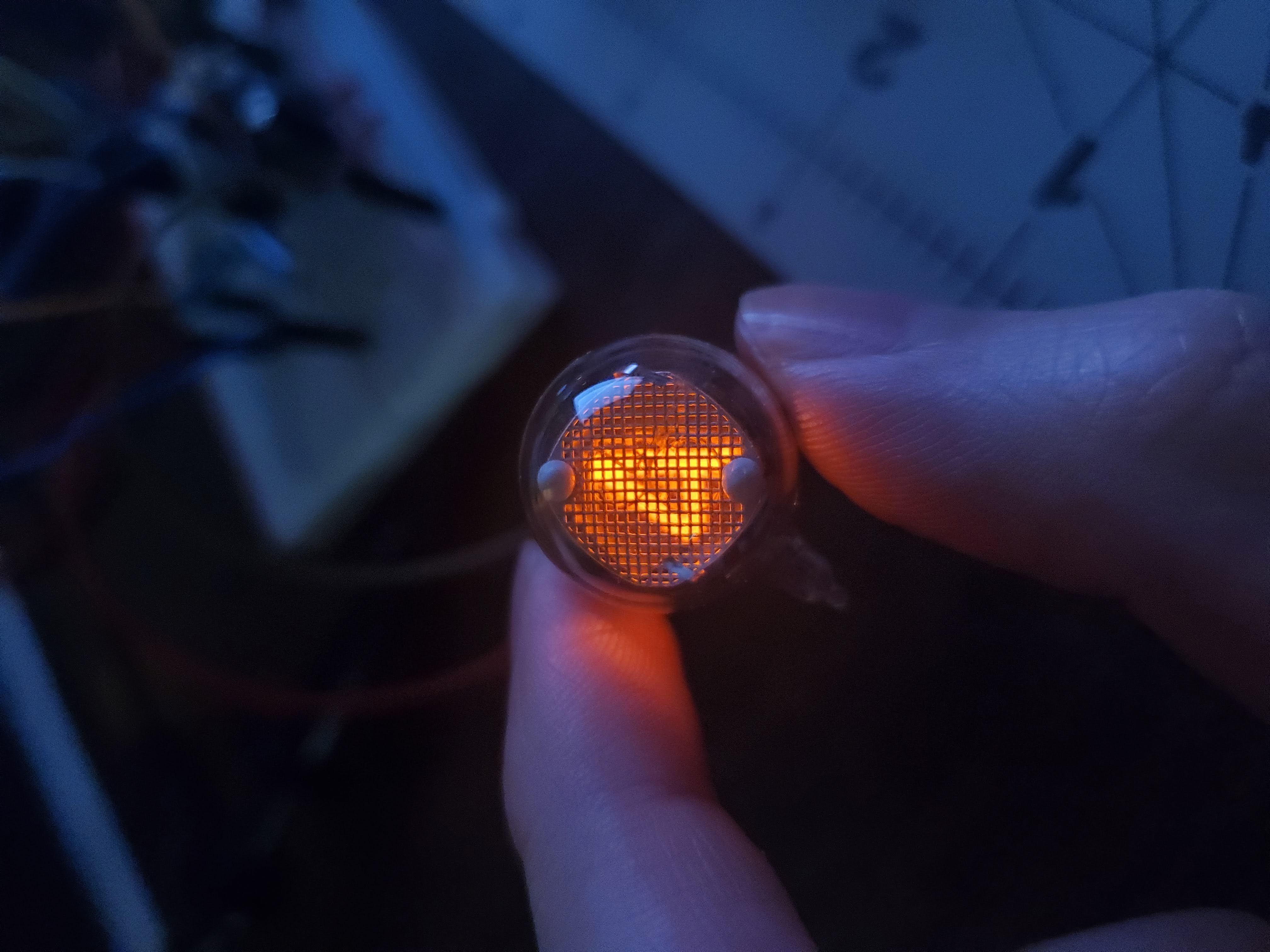
I started with a design using the common 555 timer chip. This circuit was easy to understand and get working, and it was able to power a small IN-2 nixie tube I got for testing! While a good way to get something working, this circuit relied on a 9V supply voltage, and I knew it was unlikely to handle higher loads (e.g. the 4 IN-12 nixies for the clock).
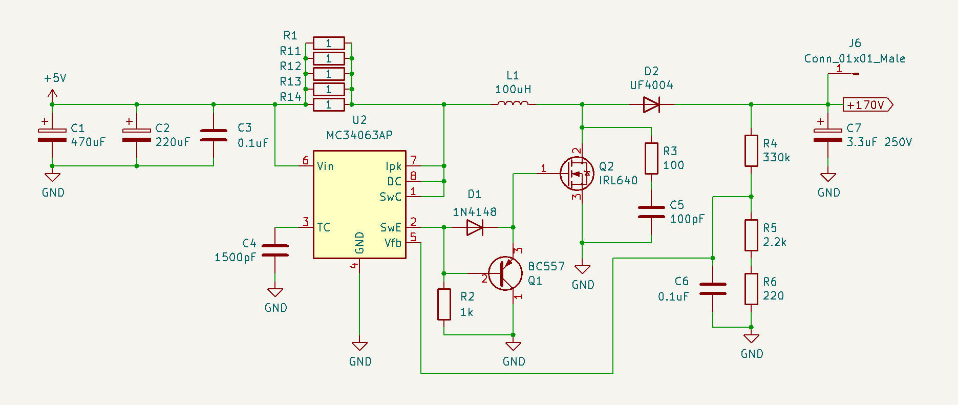
MC34063
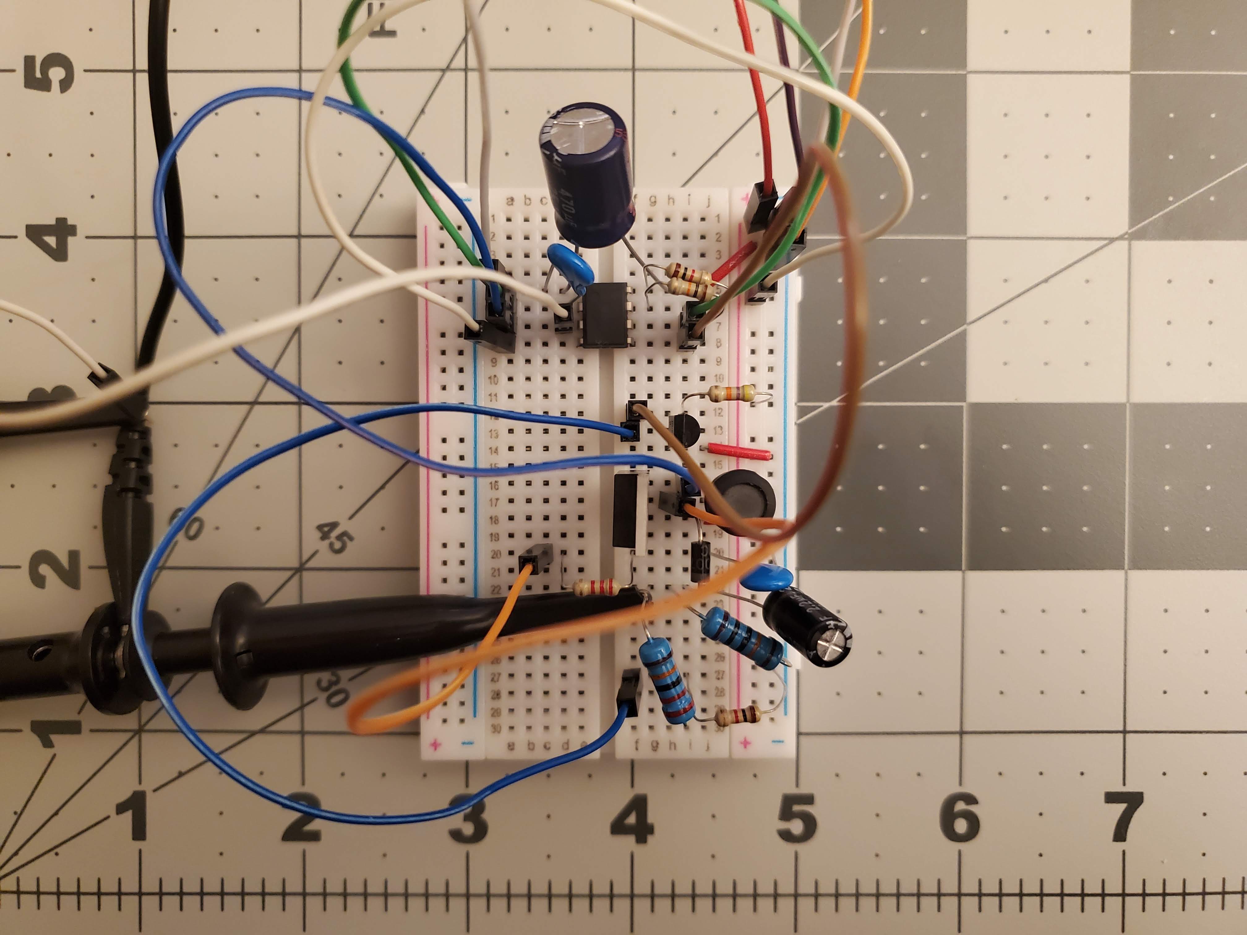
For the next iteration, I switched to a design using the MC34063, another common chip specifically made for buck / boost converter applications.
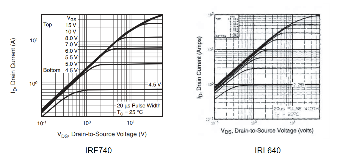
One challenge was to get this working with a supply voltage of 5V. The original design used an IRF740 mosfet, but its drain current is too low at a gate-source voltage of 5V (or ~4.2V due to the diode in the active-pulldown on the gate). I swapped this out for an IRL640 mosfet, which has a much higher drain current at this voltage:
 |
|---|
| The drain current charts of the IRF740 vs IRL640 mosfets |
One downside is that the IRL640 is rated for a max drain-source voltage of 200V vs the 400V of the IRF740, giving less buffer. However, I had trouble finding another suitable transistor, and I figured this was fine for a hobby project.
Another (self-inflicted) challenge I ran into was related to the MC34063’s sense pin. Essentially, the chip will limit current based on the voltage on this pin, which can be adjusted via a resistor value. The combination of variance in my 1ohm resistors and added resistance of the breadboard contacts meant that the current limiting was triggering when I didn’t want to - this took me a while to debug. With that fixed, I was finally able to supply more than 10mA at ~165V, which was good enough for the planned 4 IN-12 nixies; this is what I used in the final design.
Other designs
While the above MC34063A design works, it’s far from efficient (I think around 50%) and probably wouldn’t support more bulbs at full brightness. From what I’ve read, a flyback converter design using a transformer instead of an inductor can be much more efficient, though this involves additional complexities in finding / choosing the right transformer. If I make another nixie tube clock with six IN-8 or IN-14 bulbs, I’ll likely look into this kind of power supply.
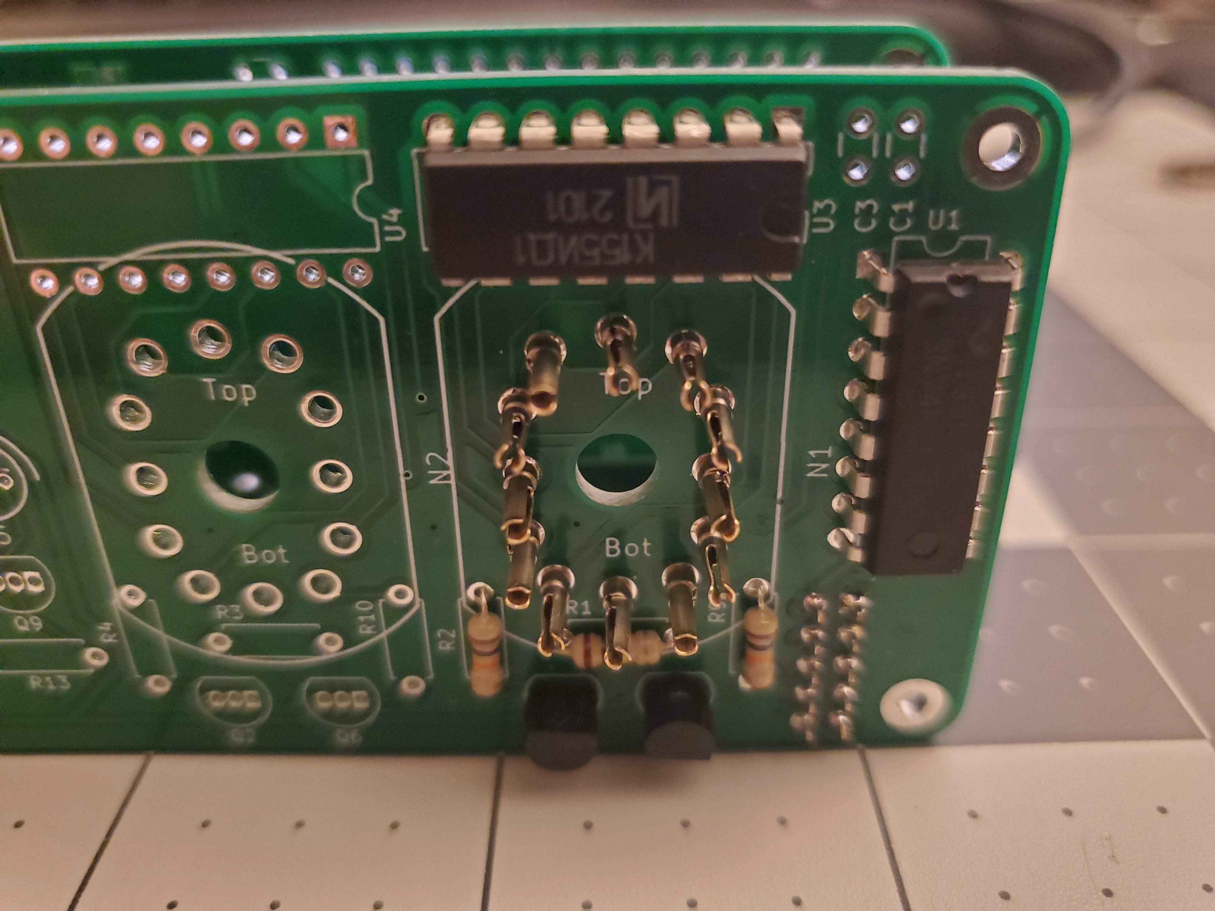
Nixie Tube Drivers
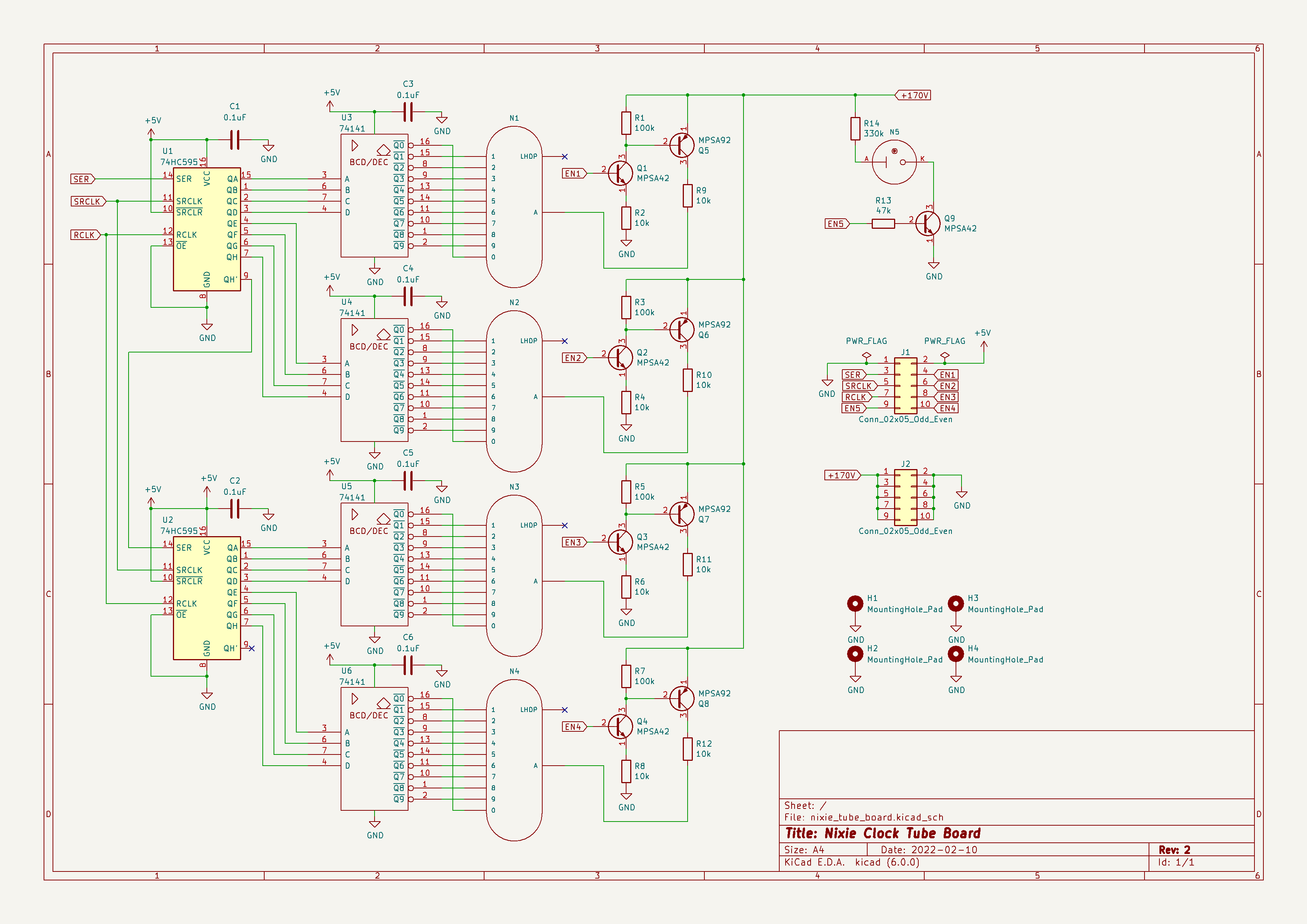
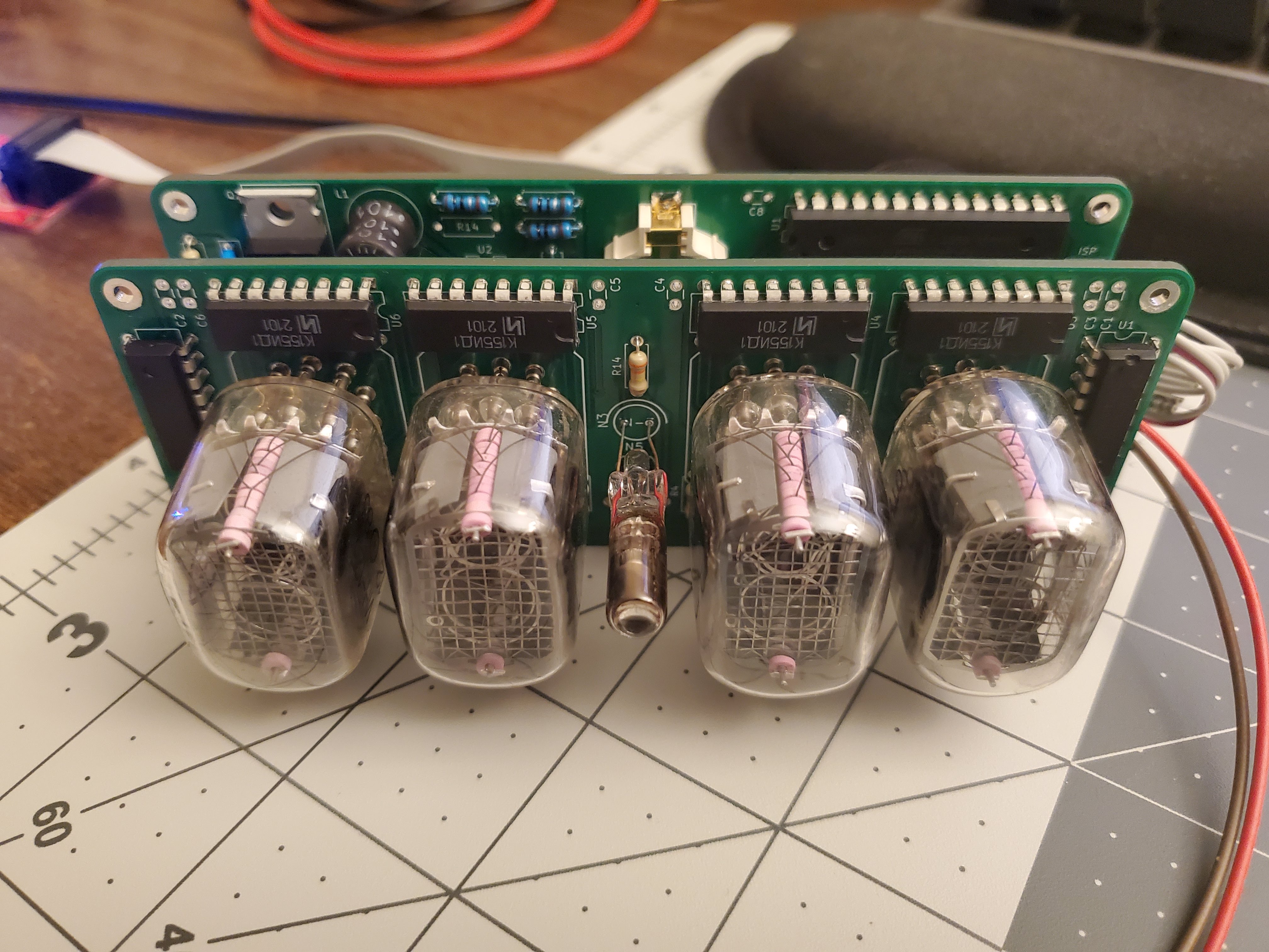
I went with the tried-and-true K155ID1 (equivalent to the 74141) to drive the 10 individual digits of each nixie tube. The K155ID1 sinks current and sits between the cathodes and ground. For simplicity, I decided to direct-drive the nixies instead of multiplexing, so there are four K155ID1 chips total (one per tube). To reduce the pins needed to control the nixies, each pair of K155ID1’s is controlled by a 74HC595 shift register. The two shift registers are wired together, allowing the microcontroller to set digits of all 4 nixies with 3 pins (serial data, clock, and enable).
To adjust the brightness, each tube has an anode side driver consisting of an MPSA42 NPN transistor and an MPSA92 PNP transistor. The INS-1 bulb is driven by a single MPSA42 NPN transistor on the cathode side.
This document is a great reference on different types of drivers; I also used circuitjs to better understand some of the designs and to pick reasonable resistor values.

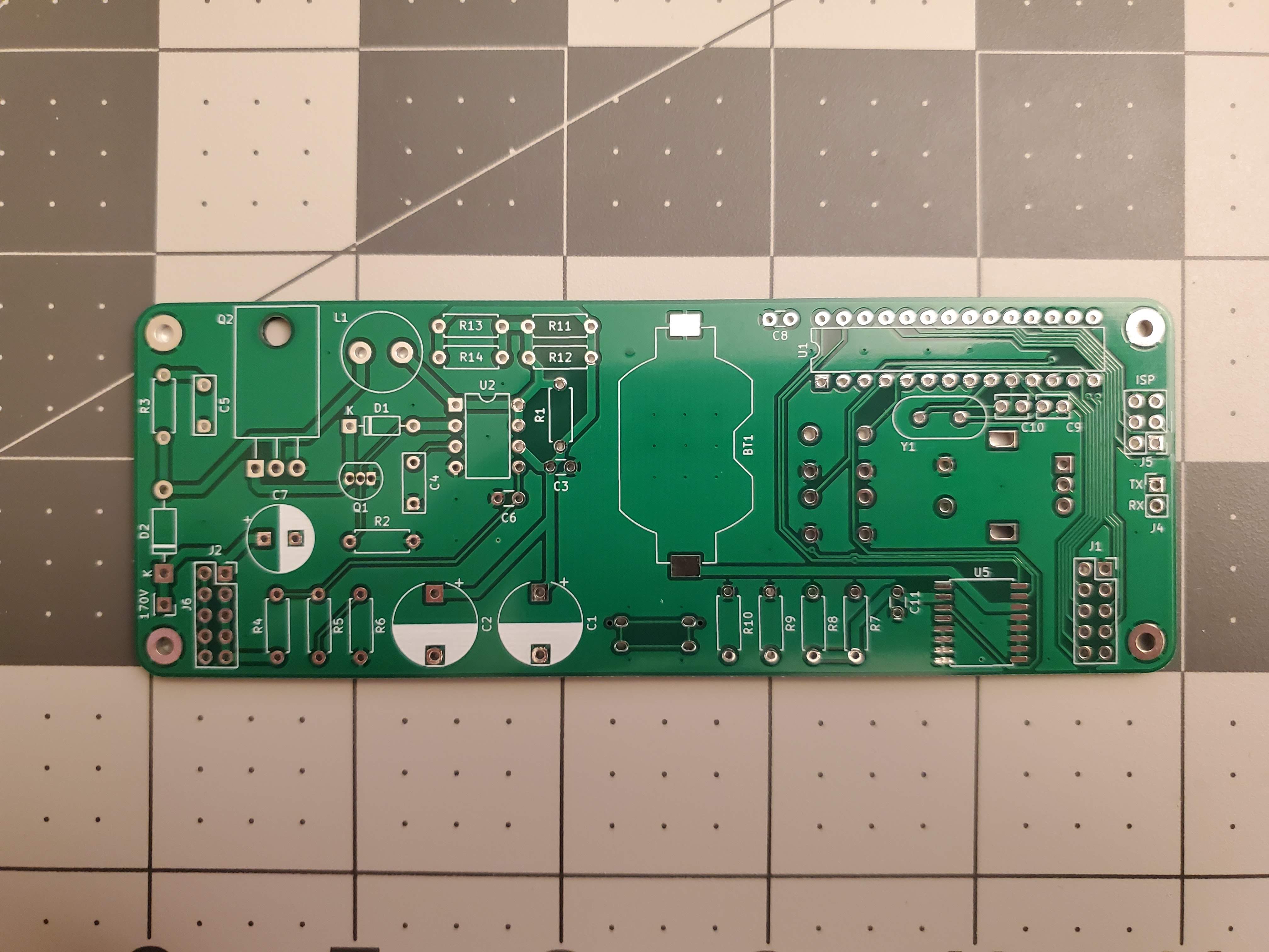
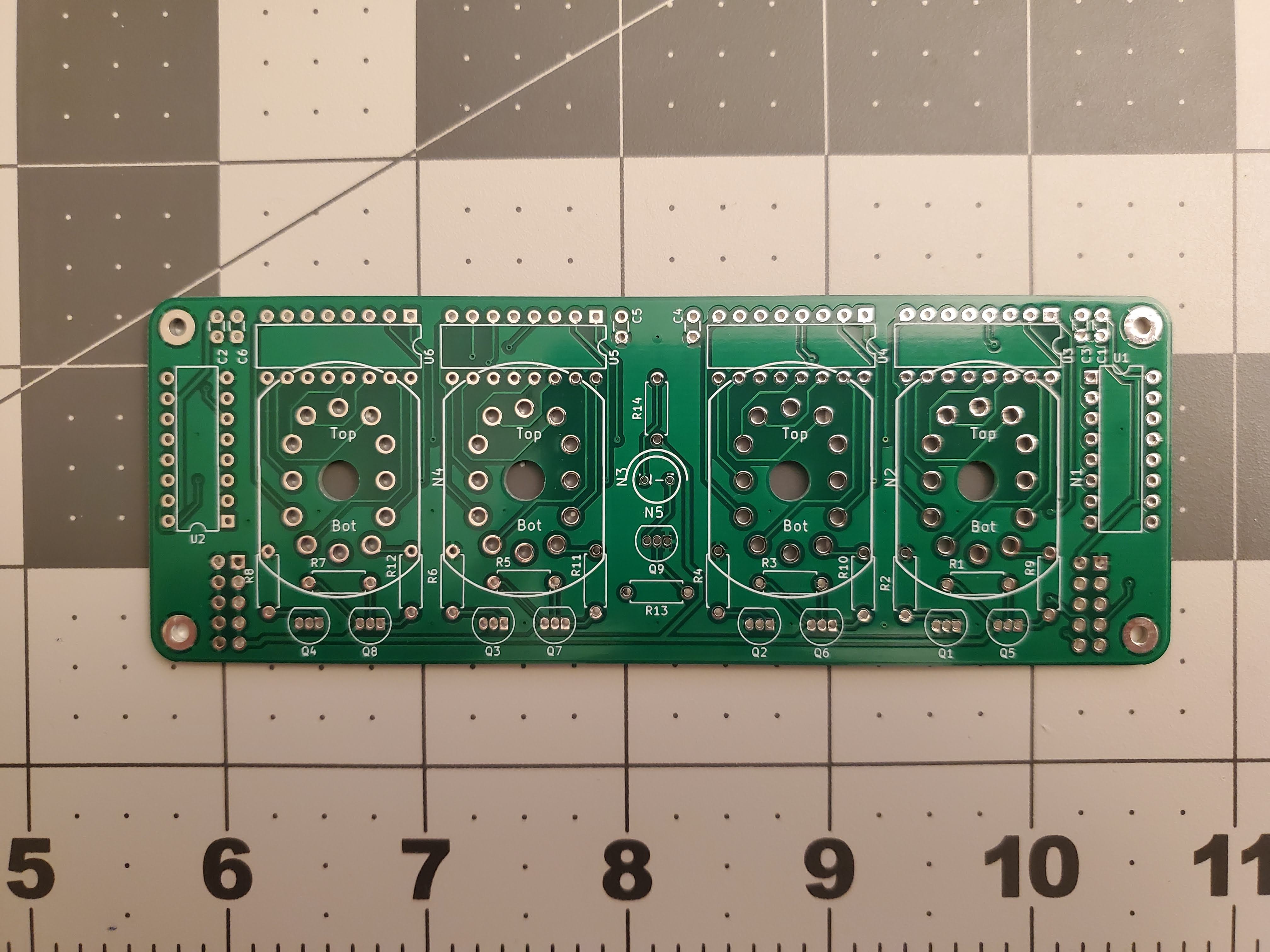
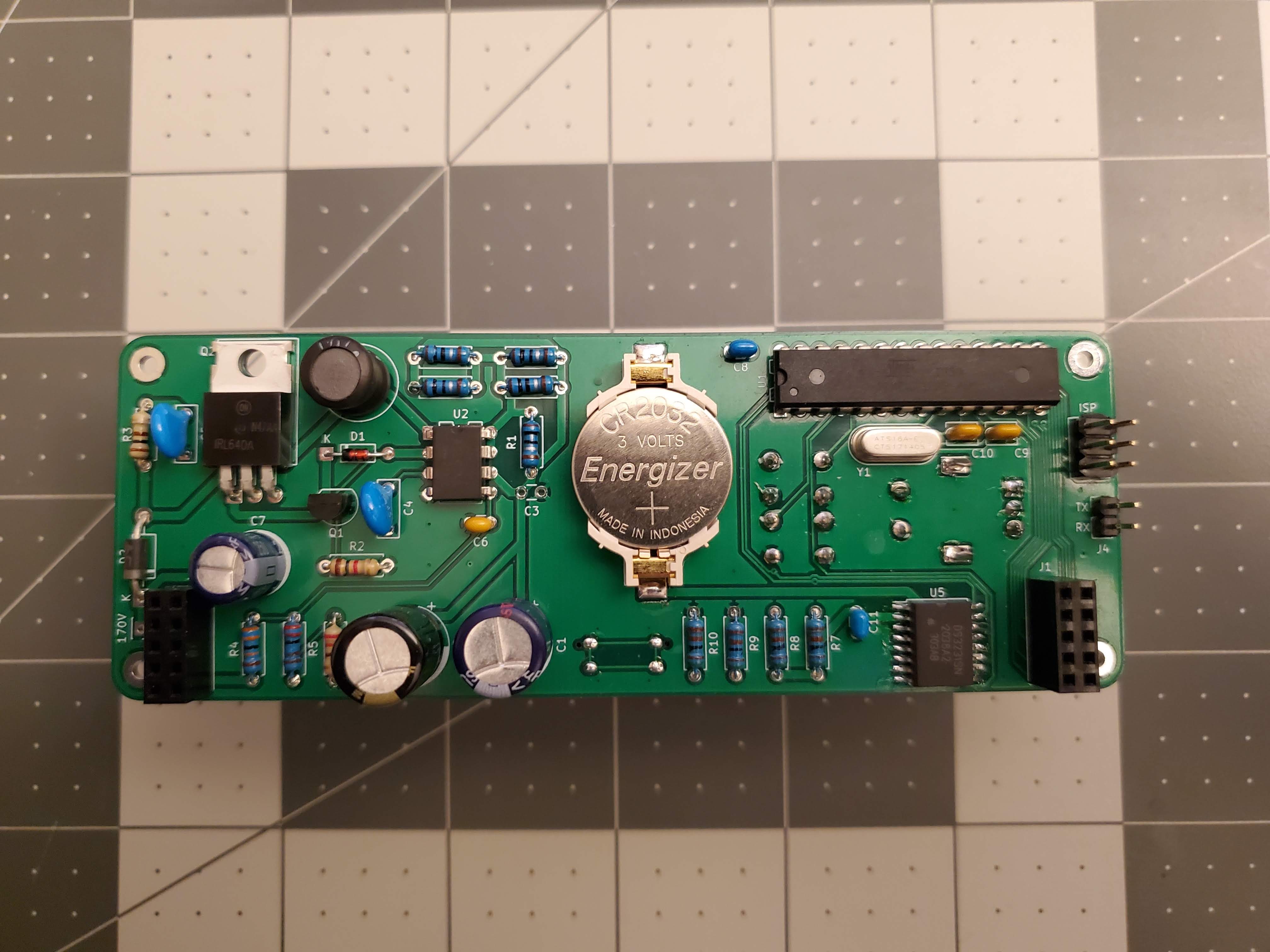
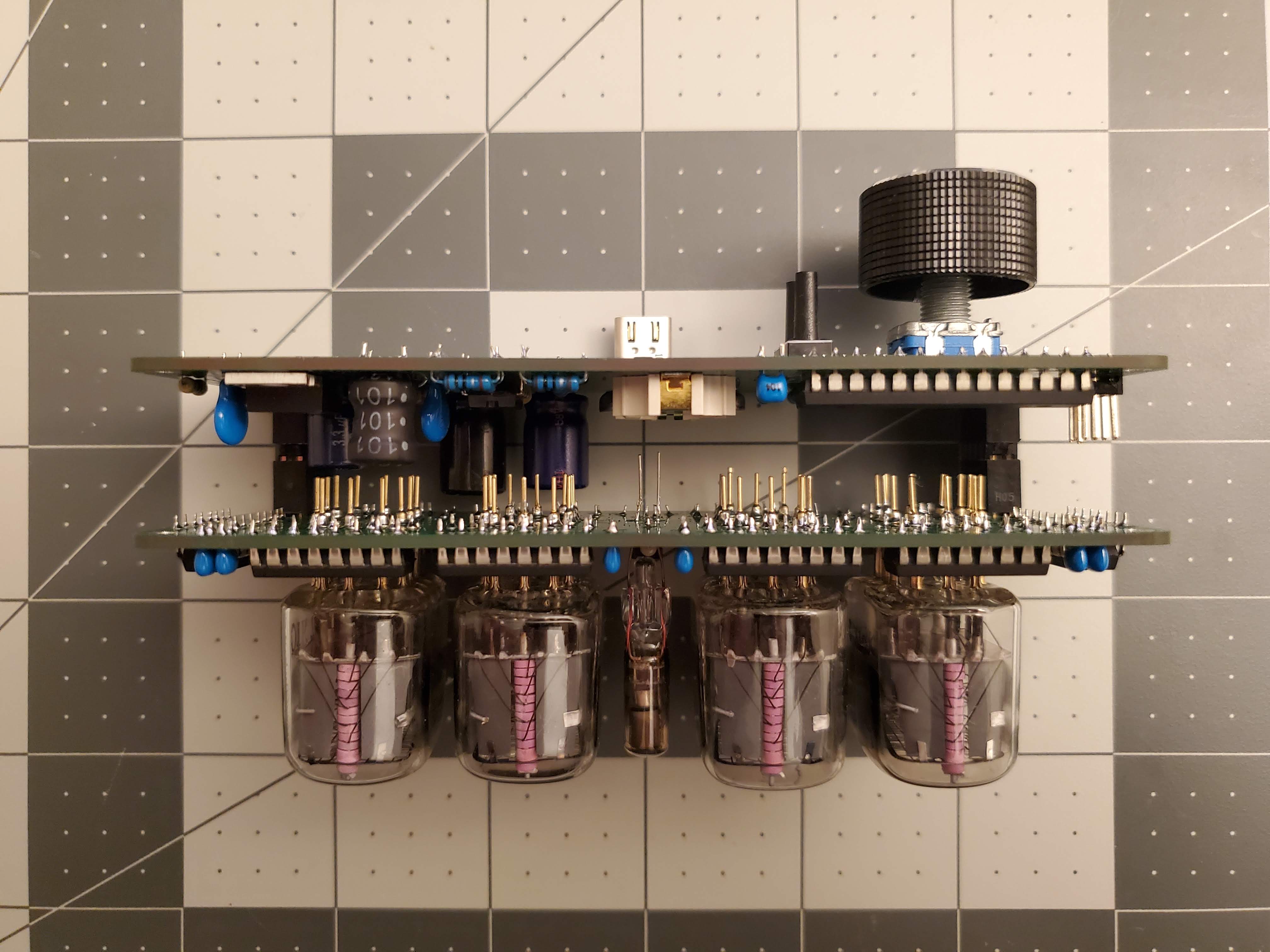
PCB Design and Assembly
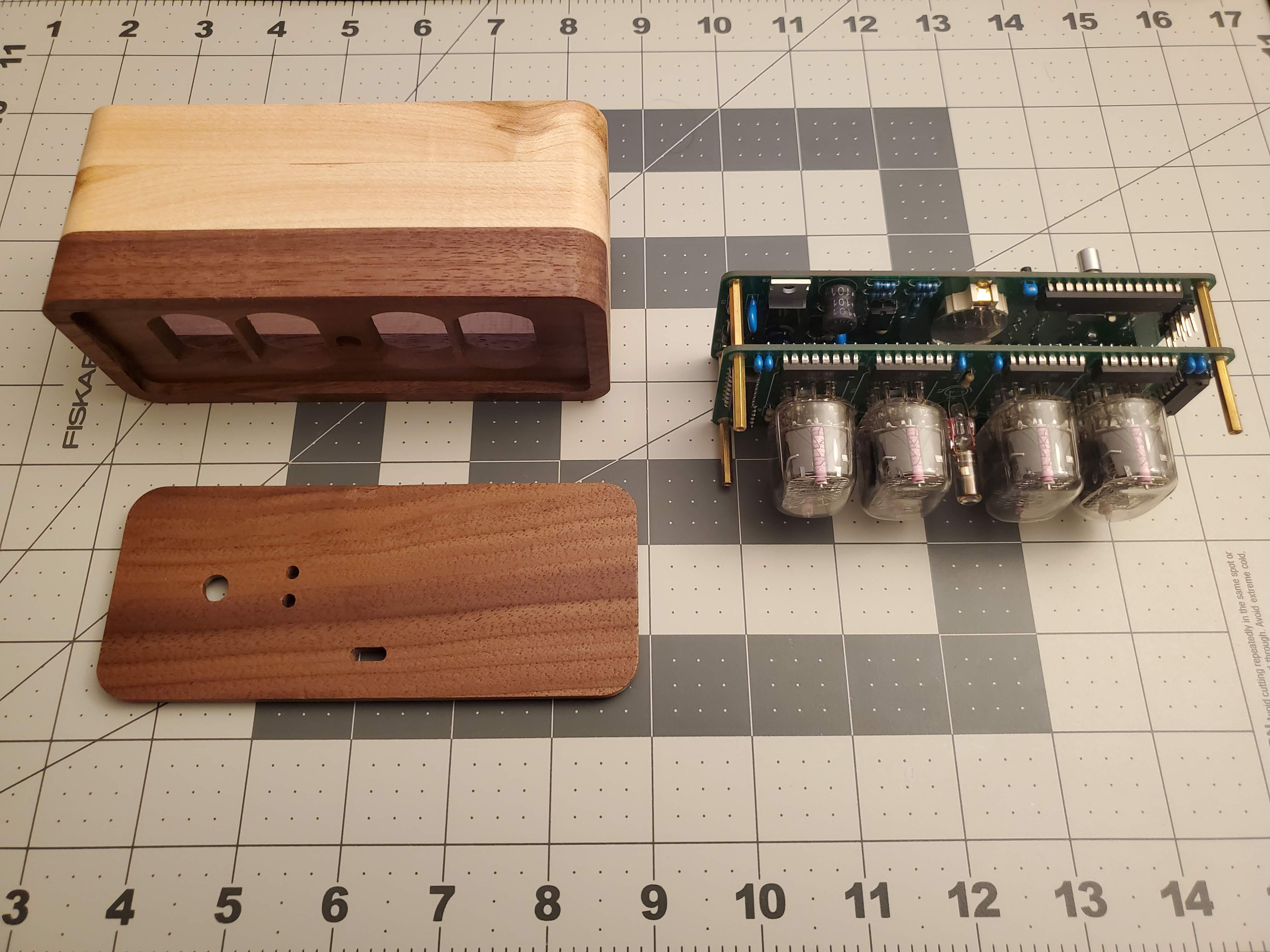
For form factor purposes, I split the clock into two PCBs to be stacked together. The main board contains the boost converter circuit, microcontroller, and RTC chip, along with the buttons and rotary encoder (attached to the back). The tube board contains the nixie tube pin connectors and driver circuitry. The boards are stacked together with a system of 5x2 female/male/female header blocks.
I used a clearance of 0.6mm for the high voltage traces and did my best to keep them on one side of the PCB. Not quite sure what the best practice is here, but it seemed to have worked fine.
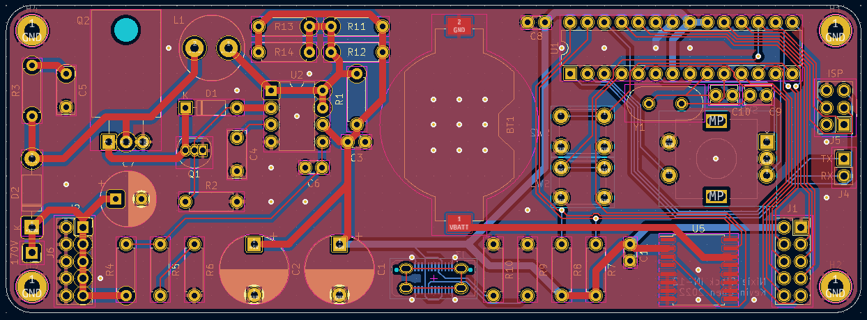
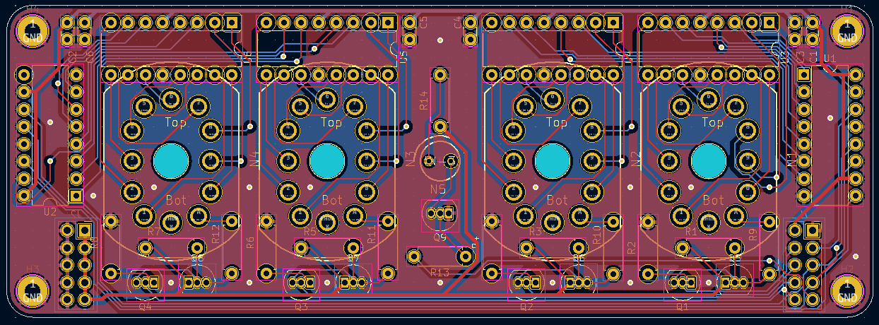
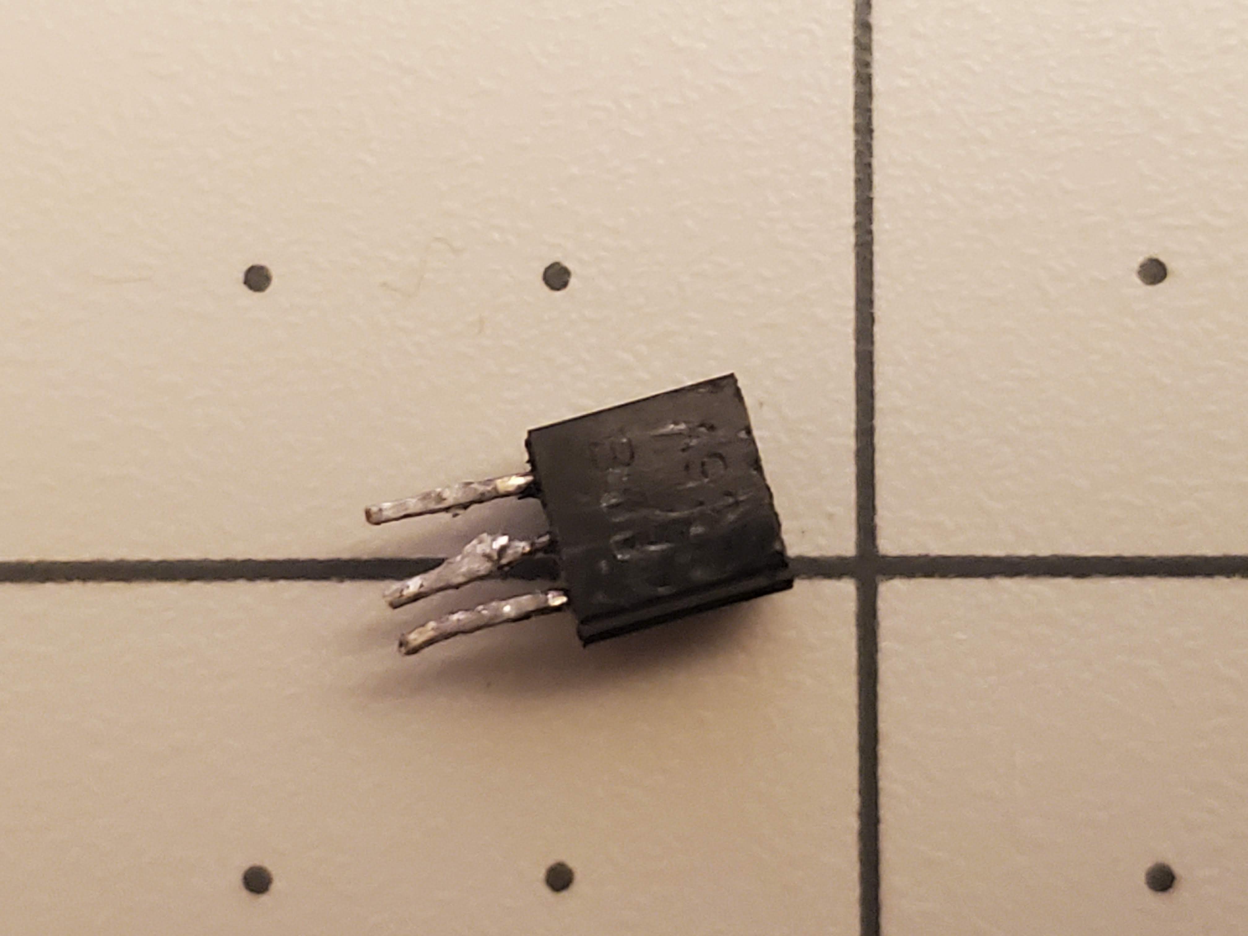
I ordered the pcbs from JLCPCB - don’t know how typical this was, but it took just 7 days to receive the order! Most components were through-hole, so assembly was fairly straightforward, though I verified that a single nixie tube worked before soldering everything. I actually did find an issue during this initial test - the orientation of the Q5 - Q8 PNP transistors is backwards; luckily it didn’t take me too long to find and only required the death of one transistor.
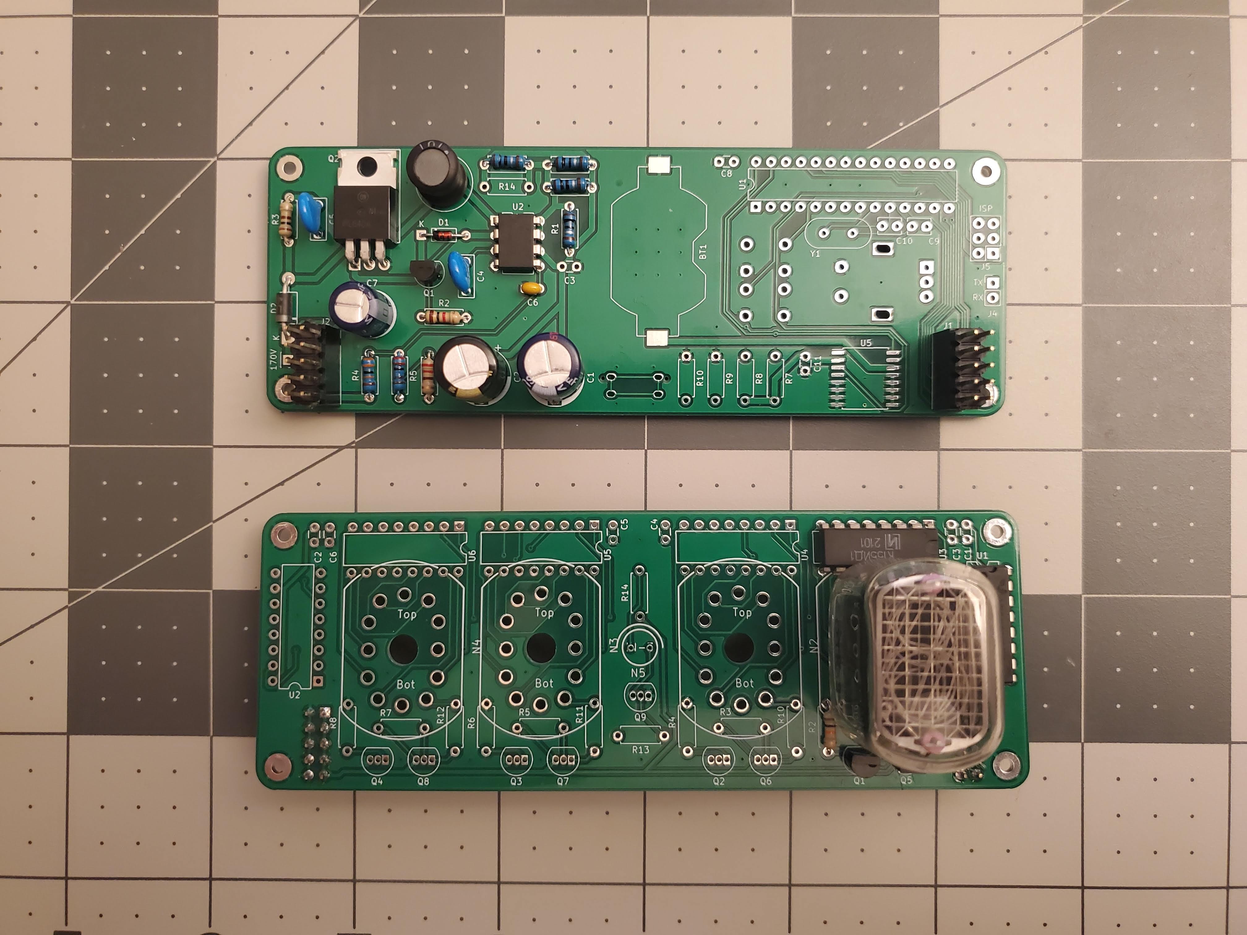
A funny story: Since I had extra pcbs and parts, I made 2 clocks. On the second clock, I messed up soldering the small pins on the USB-C connector and shorted CC1 and VBUS. Fortunately, this wasn’t catastrophic and the clock still works, but only for one orientation of the usb cable. Behold, a non-symmetric USB-C socket!
Another mistake on the second clock is that I accidentally soldered two of the nixie tubes into their pin connectors, so they’re sadly no longer removable.
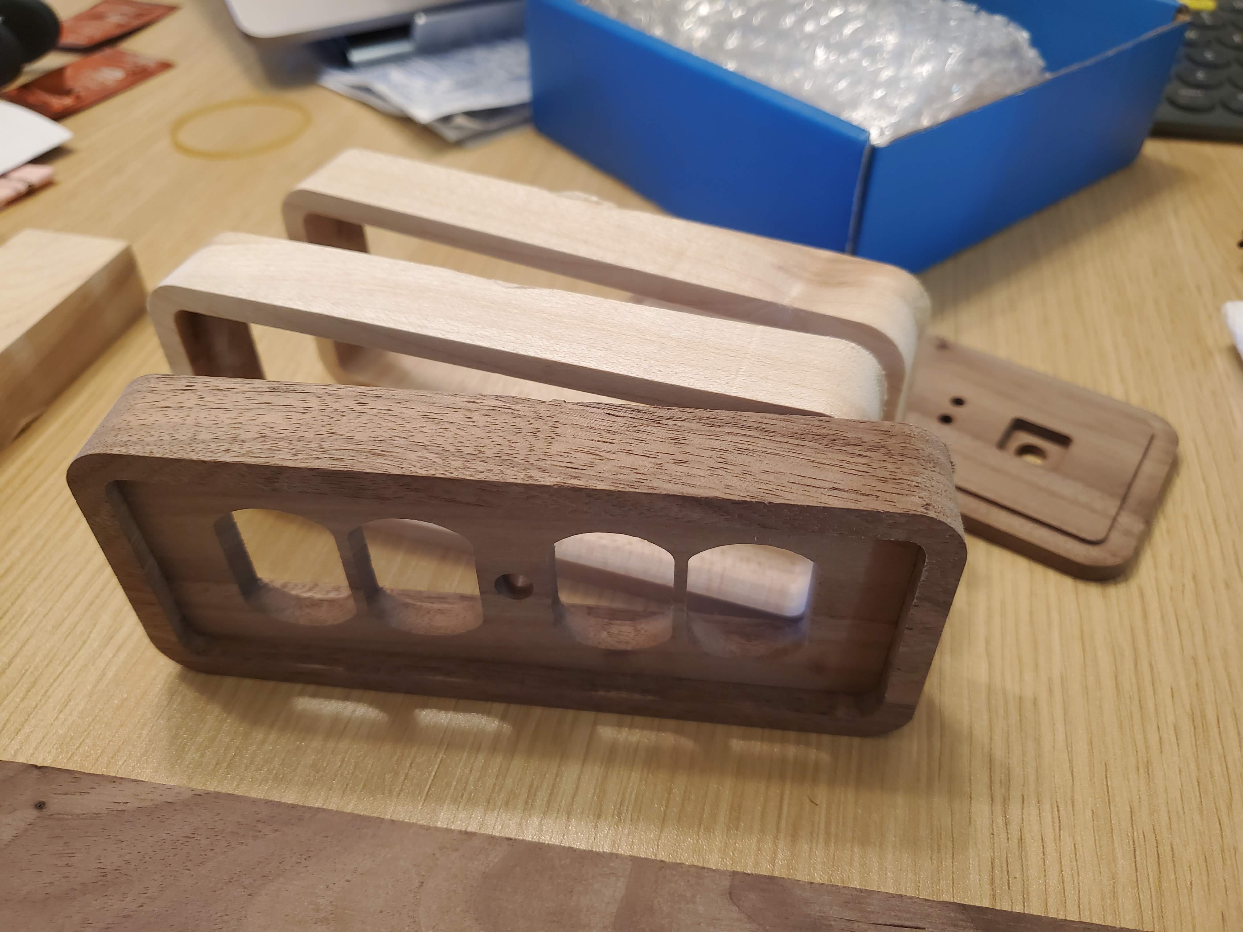
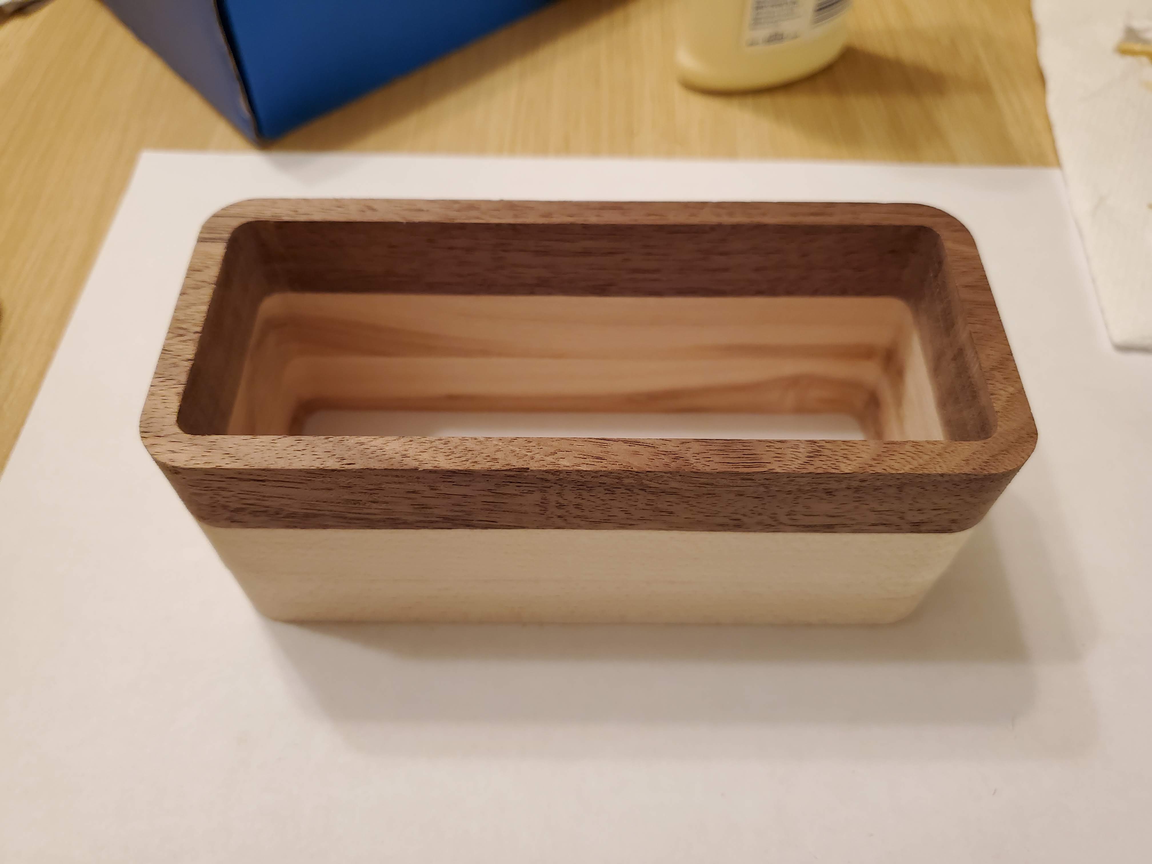
Enclosure
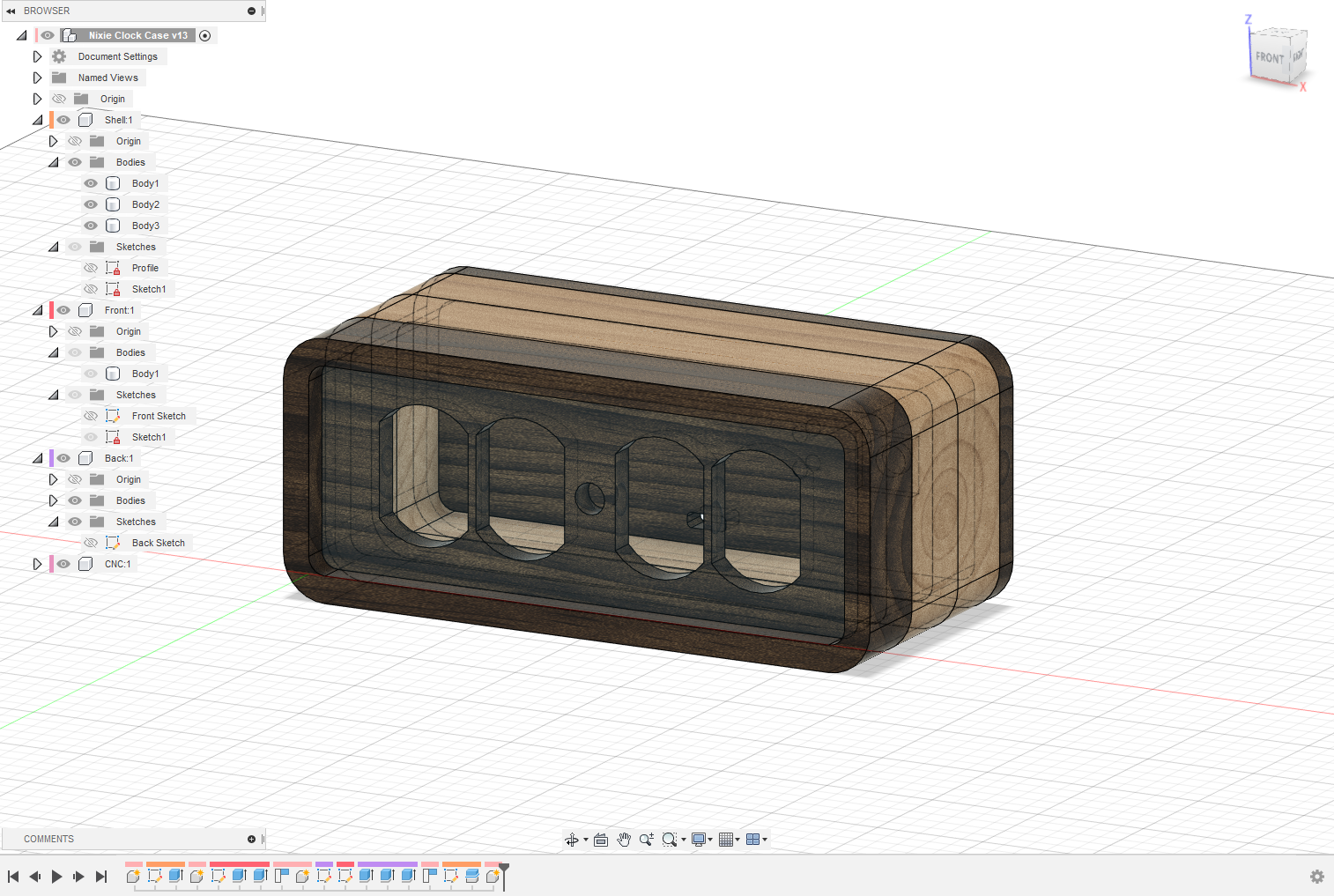
The other big part of this project was creating the wooden clock enclosure. I designed the enclosure in Fusion 360, and it consists of 5 pieces:
- 3 outer shell pieces
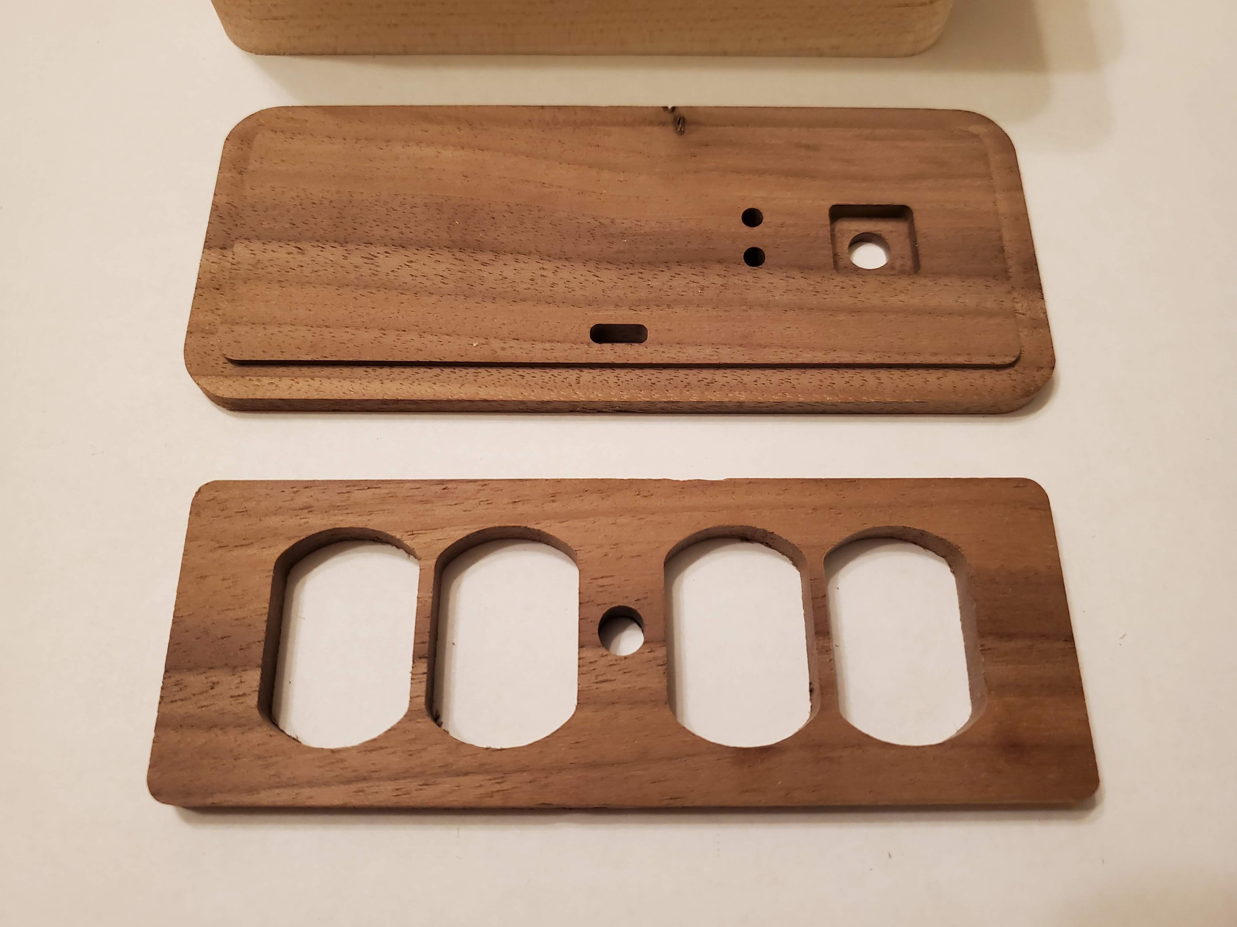
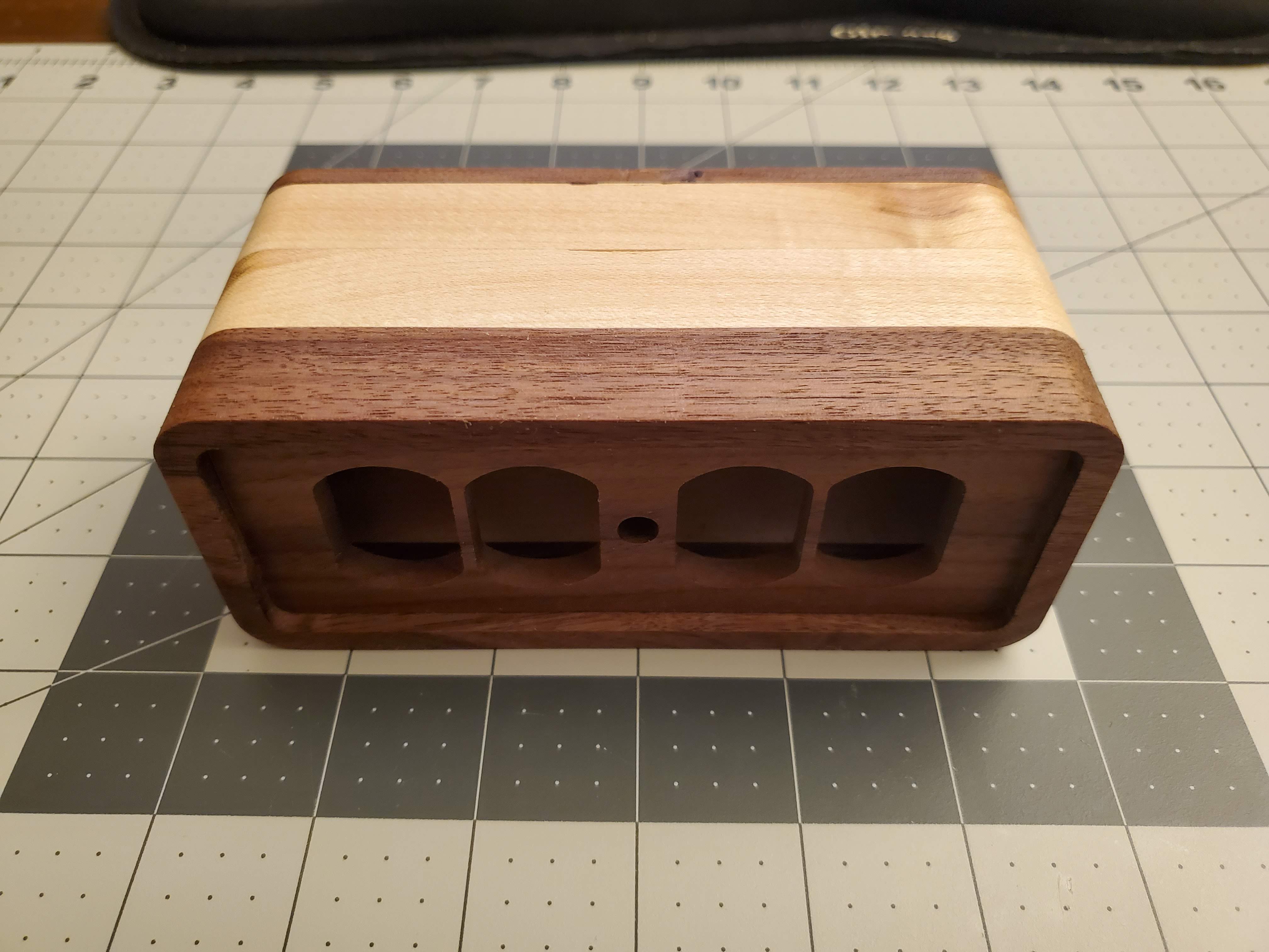
- A front plate with cutouts for the nixie tubes
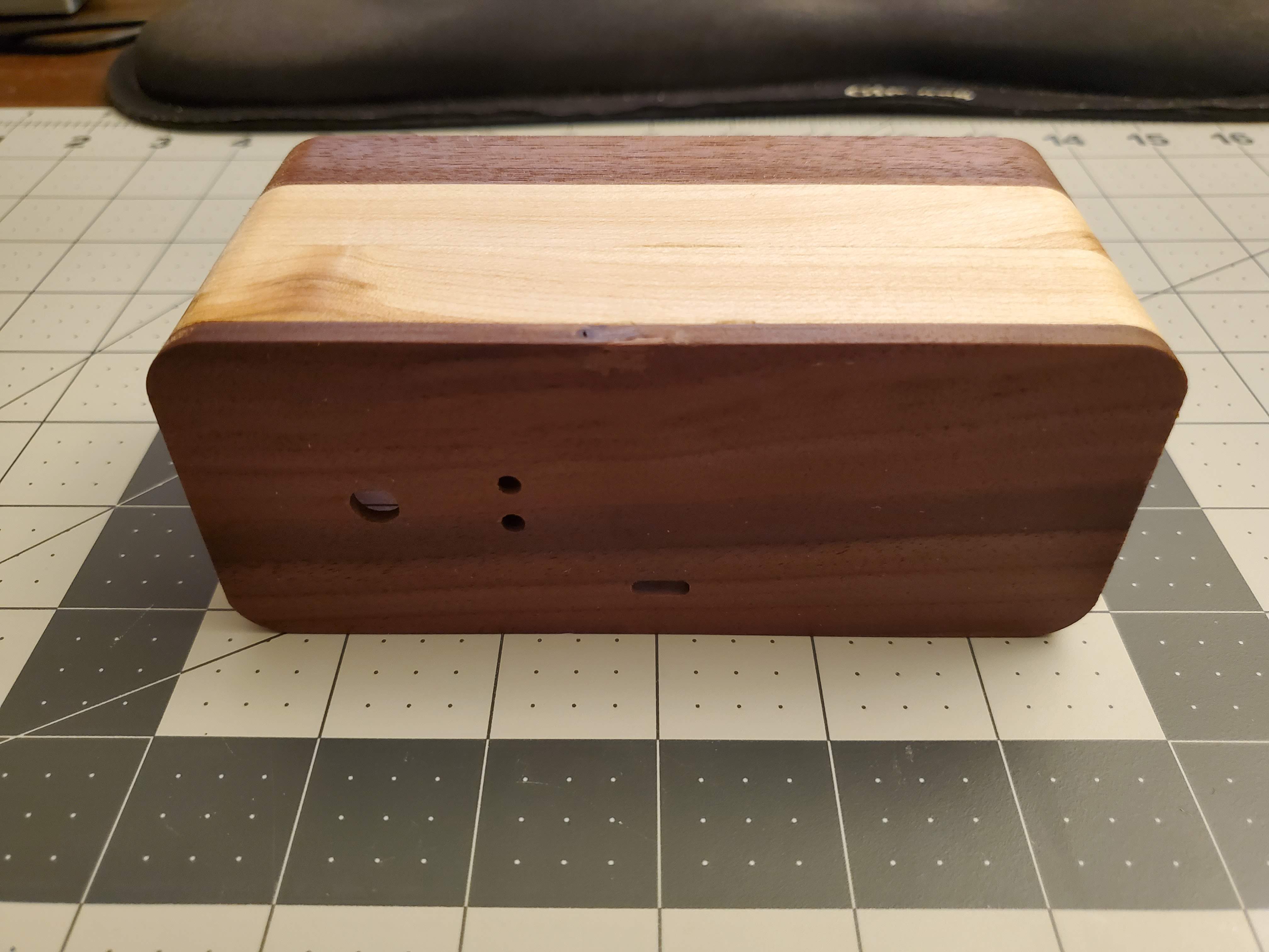
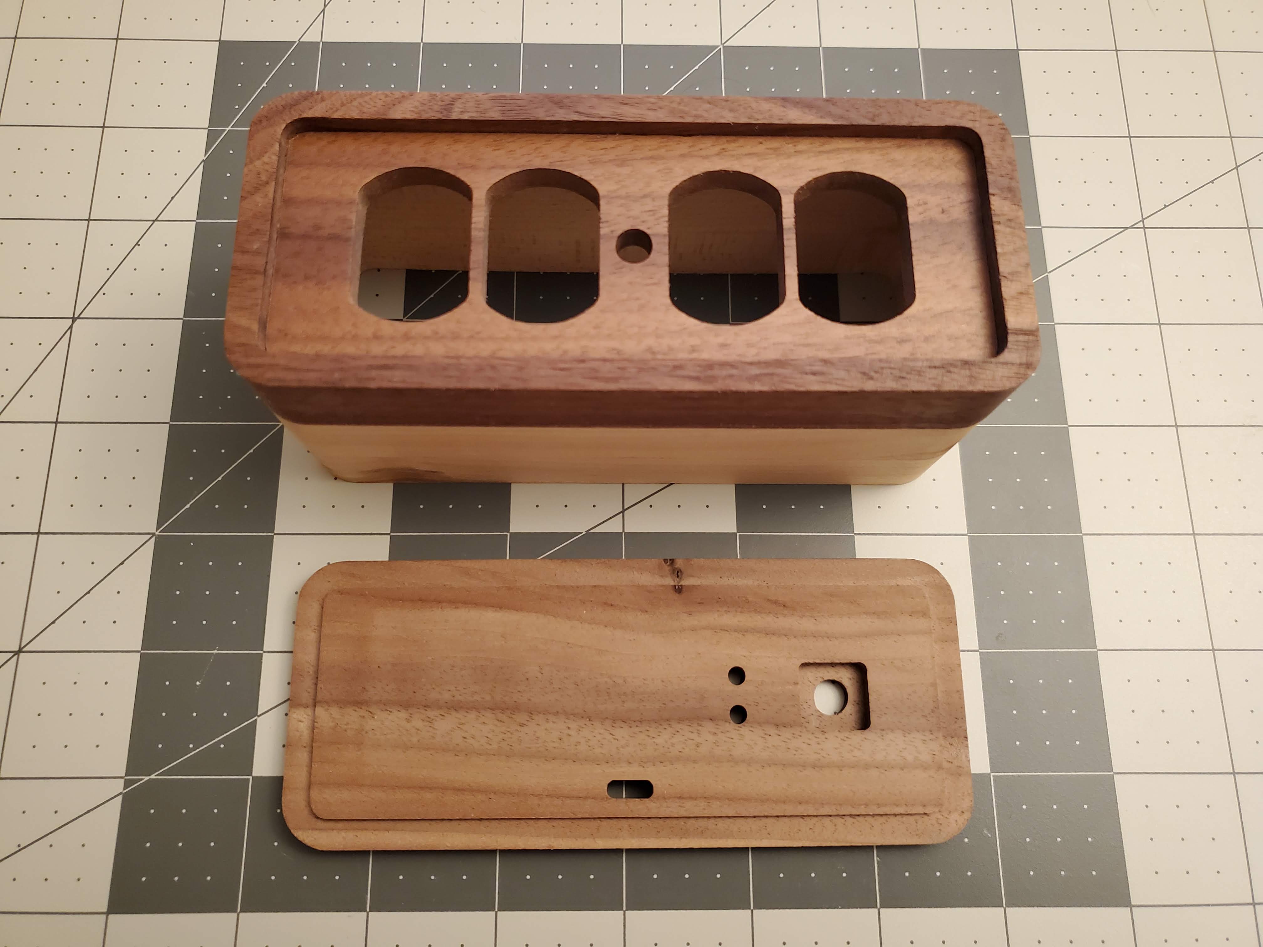
- A back plate with cutouts for the buttons, rotary encoder, and USB connector
The outer shell pieces are designed to be cut from 3/4” thick boards of walnut and maple; the front/back plates from 1/4” thick walnut. I used DXF files from the KiCAD PCB design to ensure the cutouts would line up.
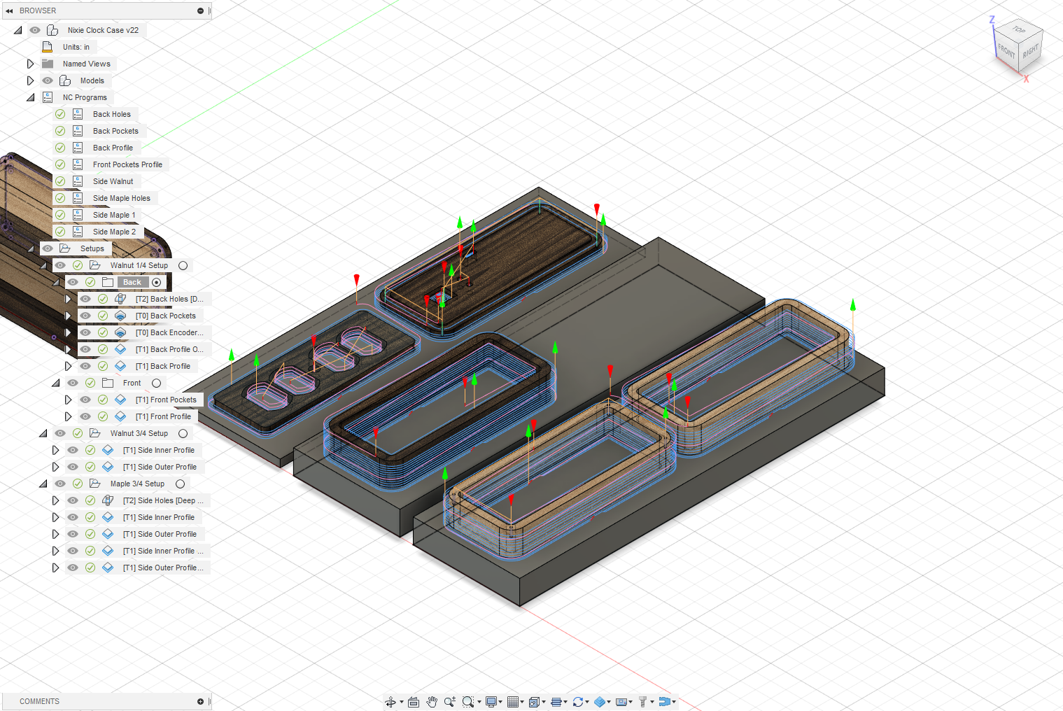
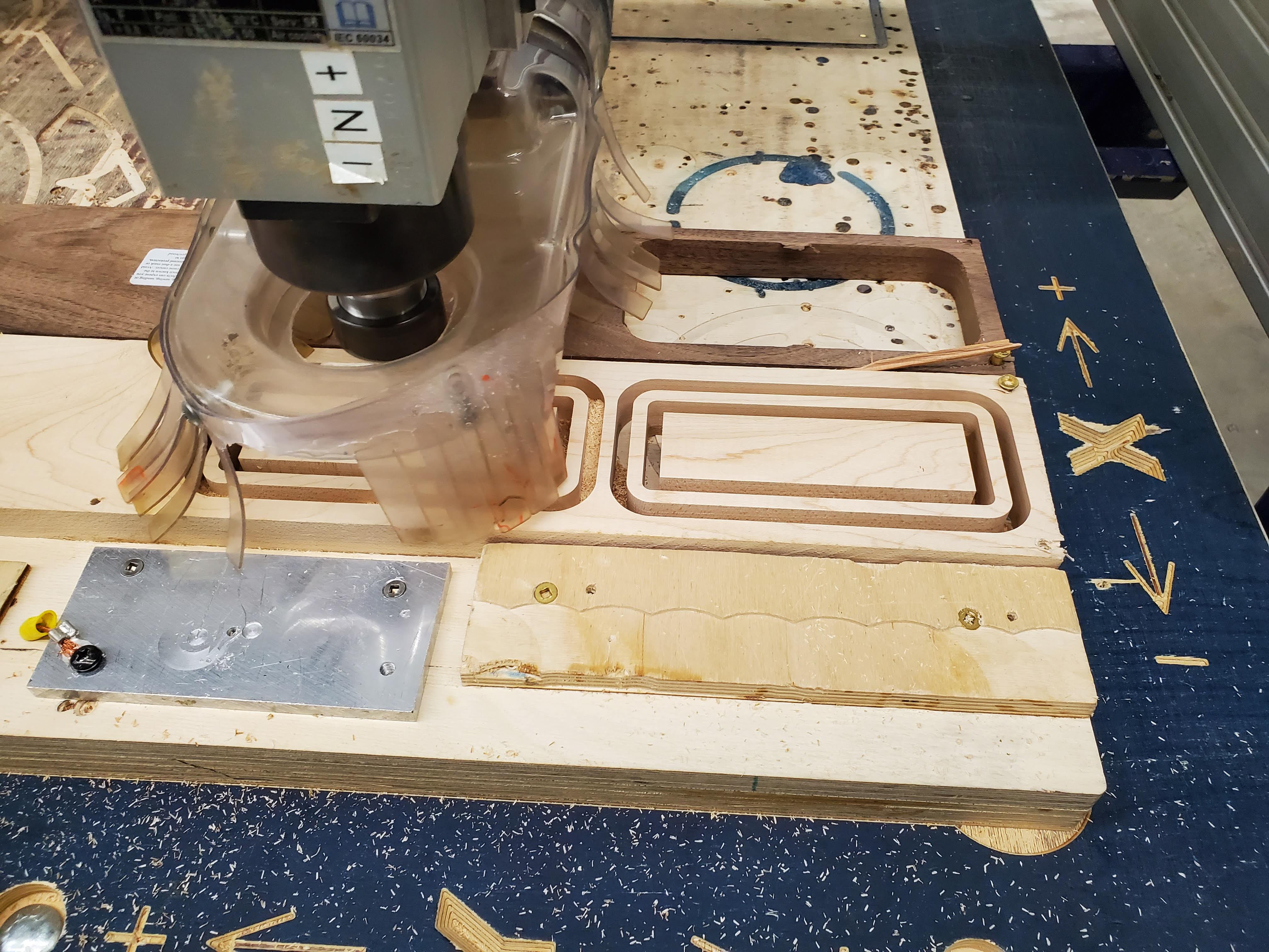
CNCing
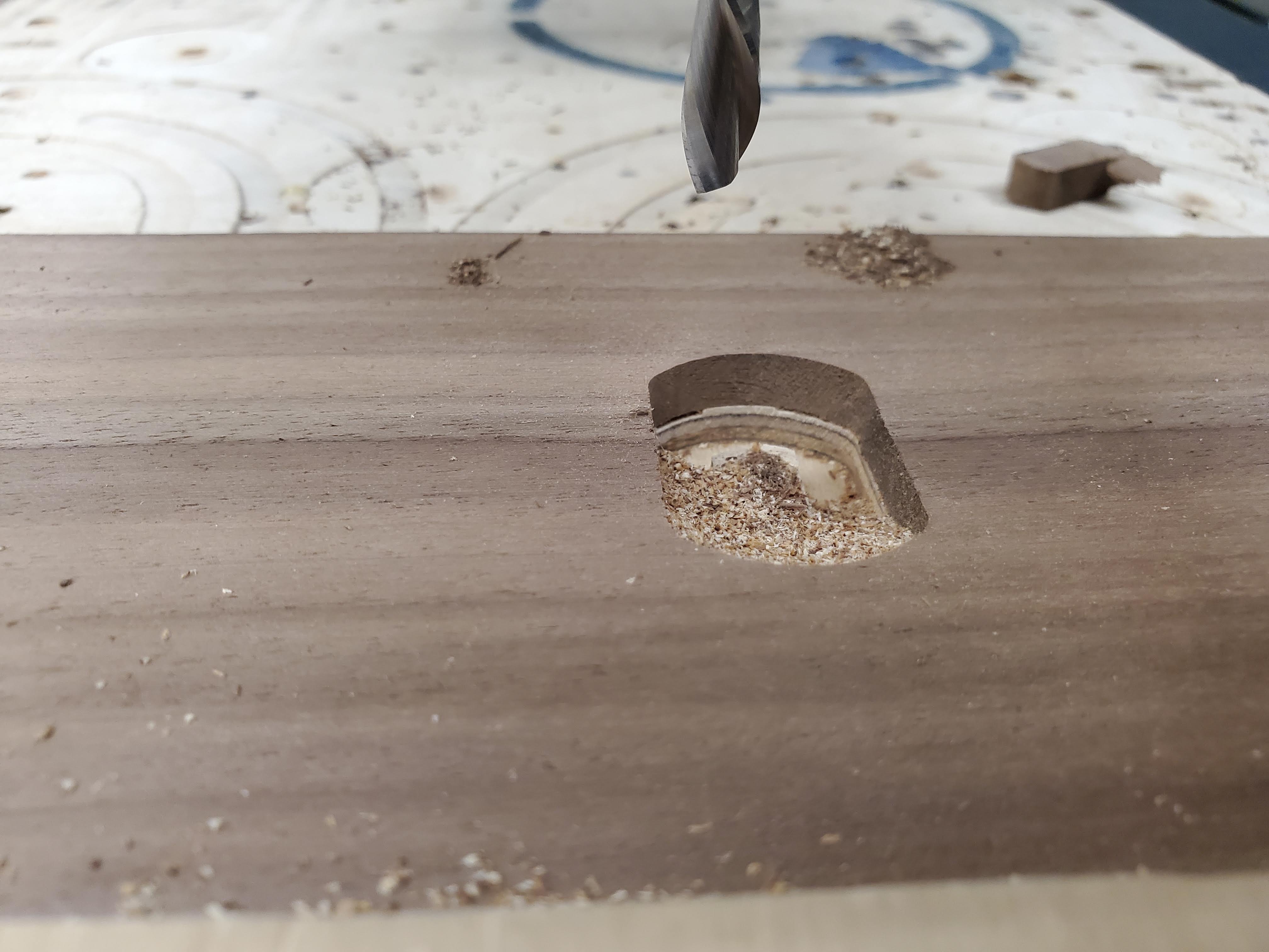
To actually create the pieces, I used a Shopbot Alpha CNC machine at my local makerspace. This was the first time I’d used a CNC, so of course I had to make the rookie mistake of incorrectly setting the Z height and cutting into the spoilboard. It wasn’t a huge deal and folks at the makerspace were incredibly understanding, but it sure was embarrasing to tell everyone I’d made the exact mistake they explicitly warn about in the intro class…
But other than that initial snafu, the CNCing went smoothly. I used 3 different bits:
- 1/4” diameter spiral downcut bit for the main profiles and nixie tube cutouts
- 1/8” diameter spiral downcut bit for the button, encoder, and USB connector cutouts
- 1/16” diameter spiral upcut bit for the back plate screw pilot holes

Assembly and Finish
Assembly was fairly simple. I first hand sanded the outside surfaces to 220 grit (also had to sand the inner shell a bit to get the PCBs to slide in more easily). I then glued the outer shells and front plate together and tapped threads for M2 bolts to attach the back plate. I used spray polyurethane for the final finish. The surface turned out rougher than I would have liked - I didn’t do the best job at hand sanding, and I think dust got caught in the poly since I applied it outdoors. If I were to do this again, I’d probably just use an orbital sander and use wipe-on poly instead.
I used brass M2 spacers and standoffs for the PCB stack. The electronics stack simply slides into the clock enclosure; it’s a tight fit and doesn’t require any fasteners to stay in place (aside from the bolts for the back plate).


Software
The clock software is fairly straightforward. At its core, it continuously queries the DS3231 chip for the current time and updates the nixie tube display as needed by writing data to the shift registers. There are 8 display states you can cycle through using the rotary encoder:
- Hour and minutes (HH:mm)
- Minutes and seconds (mm:ss)
- Date (MM:dd)
- Year (yyyy)
- Brightness setting
- 12 or 24 hours setting
- De-poison period setting
- De-poison
The separator dot is also toggled every second in the HH:mm and mm:ss states. The brightness of each digit is controlled via hardware PWM with timers configured to run at 976.5 Hz.
Edit Mode
Pressing the top pushbutton will enter edit mode for the current display state. In this mode, rotating the encoder changes the selected value and pressing the encoder cycles which value you are editing (e.g. hours or minutes). Pressing the top pushbutton will save your changes and leave edit mode, while the bottom pushbutton will ignore any changes and leave edit mode.
- Editing the first 4 states changes the current date or time, which gets written back to the DS3231
- The brightness setting controls the display brightness from 1 - 9
- The 12 or 24 hours setting controls if the HH:mm display is 12-hour or not
- The de-poison period setting controls how often run the de-poison routine (every 15, 30, 60 minutes, or never)
The settings are stored to EEPROM so are preserved on loss of power.
De-Poisoning
Cathode poisoning is a known phenomenon with nixie tubes - this is when the inactive digits get increasingly coated with resistive sputtered material, reducing their ability to glow. In a clock, this is primarily a concern for the leftmost tube, where the 3-9 digits generally remain unused. One way to counter this is to periodically ignite all digits of a tube to burn off any built-up coating.
The clock uses a periodic de-poison routine to do this. At a configurable interval (every 30 minutes by default), the display will turn to max brightness and cycle through random digits on all bulbs for 25 seconds. The animation pattern is roughly based on the divergence meter from Steins;Gate: